
The ASML Monopoly: Why Lithography is the Hardest Problem in Tech

To understand why the global semiconductor industry hinges on a single Dutch entity, one must first appreciate the staggering physics of Extreme Ultraviolet (EUV) lithography. At its simplest, chip manufacturing is a process of photolithography—projecting light through a stencil to print circuits onto silicon wafers. However, as we have squeezed billions of transistors onto chips the size of a fingernail, the wavelength of light used to etch those patterns has become a fundamental physical barrier. While Deep Ultraviolet (DUV) machines use 193-nanometer light, EUV technology slashes this wavelength down to an incredibly precise 13.5 nanometers. This shift is not merely an incremental improvement; it is the difference between drawing with a thick marker and using a focused laser to etch a single atom’s width, enabling the production of the 5nm and 3nm chips that power today’s most advanced AI processors and smartphones.
The engineering required to harness this light is nothing short of miraculous, as EUV photons are so fragile that they are absorbed by almost everything—including air. Consequently, the entire lithography process must occur within a near-perfect vacuum, requiring machines that are essentially giant, precision-engineered metal cathedrals. The light source itself, developed by ASML’s subsidiary Cymer, involves firing high-power lasers at droplets of molten tin falling at high speeds, creating a plasma that emits the necessary EUV radiation. Furthermore, because traditional glass lenses would absorb EUV light, ASML had to partner with Zeiss to engineer the world’s flattest mirrors. These mirrors are so perfectly smooth that if they were scaled to the size of Germany, the largest bump would be less than a millimeter high. This level of precision is not just expensive; it is a manifestation of decades of iterative, hyper-specialized global collaboration.
The complexity of an EUV machine is such that it contains over 100,000 components, sourced from thousands of specialized suppliers across the globe, making it perhaps the most intricate machine humanity has ever built.
The reason ASML remains untouchable, and why building a domestic clone is such a daunting prospect for any nation, lies in this deeply entrenched supply chain. ASML does not merely “manufacture” these tools; they act as the primary architect of a global ecosystem where every component—from the specialized sensors to the vibration-dampening foundations—must operate in perfect, sub-nanometer harmony. Attempting to replicate this requires more than just capital or state-led industrial policy; it demands the synthesis of breakthroughs in materials science, optics, and software that have been refined by thousands of engineers over thirty years. Until a competitor can effectively replicate the entire chain of specialized sub-suppliers and the decades of institutional knowledge embedded in ASML’s design, the company will continue to hold the keys to the future of high-performance computing.
The Anatomy of an EUV Machine: A Symphony of Physics
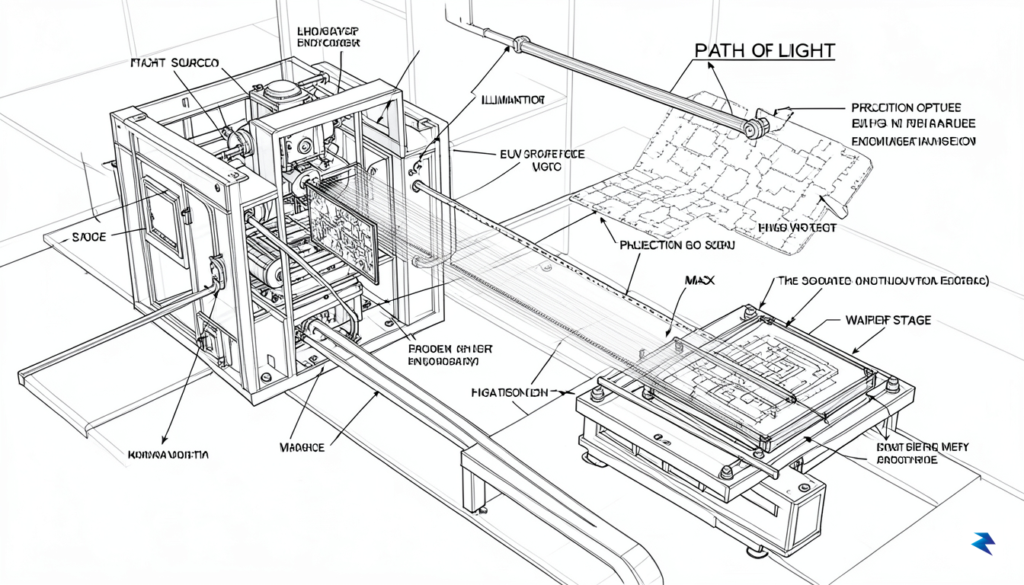
The journey from a blueprint to a functional Extreme Ultraviolet (EUV) lithography machine is less about assembly and more about an intricate dance between disparate scientific disciplines, each pushed to its absolute limits. It’s a testament to human ingenuity, requiring simultaneous mastery over fields ranging from plasma physics to atomic-scale optics, all operating within an environment of unimaginable precision. This confluence of challenges makes replicating such a system a monumental, almost insurmountable, task.
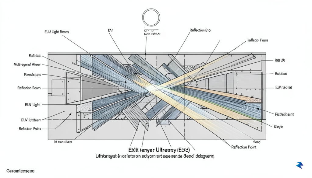
One of the most astonishing components is the light source itself, an engineering marvel known as the tin-droplet laser system. To generate the specific 13.5-nanometer wavelength EUV light required for printing, a high-power CO2 laser fires two pulses in rapid succession at microscopic droplets of molten tin, each smaller than a human hair, as they free-fall through a vacuum chamber. The first pulse pre-shapes the droplet, while the second vaporizes it into a superheated plasma that emits EUV radiation. This process occurs tens of thousands of times per second, demanding unparalleled synchronization and control over droplet generation, laser timing, and the subsequent collection of the ephemeral light, all while meticulously managing the highly corrosive tin debris to prevent damage to the delicate internal components.
Beyond the light source, the manipulation of EUV light presents another layer of profound difficulty. Unlike visible light, EUV is absorbed by nearly everything, including air and conventional mirrors. This necessitates an ultra-high vacuum environment throughout the machine and the use of specialized ‘Bragg’ mirrors. These aren’t your typical reflective surfaces; instead, they are engineered with hundreds of alternating layers of silicon and molybdenum, each only a few nanometers thick. These layers are precisely deposited to create constructive interference, allowing a remarkable (though still not perfect) 70% reflection of the EUV light per mirror. Manufacturing these mirrors, particularly the large, complexly curved ones, to atomic-level smoothness and layer thickness uniformity over vast areas, is an art form in itself, requiring precision that verges on the impossible.
Furthermore, the entire system operates under tolerances that defy conventional engineering. The wafer stage, which holds the silicon wafer being patterned, must be positioned and moved with nanometer accuracy, even as it accelerates and decelerates rapidly. This is equivalent to moving an airplane from New York to Los Angeles and hitting a specific spot within the width of a human hair. Any vibration, even from distant traffic, or a minuscule temperature fluctuation of a fraction of a degree Celsius, can cause components to expand or contract just enough to ruin the exposure. The optical alignment within the machine must be maintained to picometer precision – a thousand times smaller than a nanometer – ensuring that the light perfectly illuminates the reticle and is then focused onto the wafer without a single micron of error. This level of environmental control, active vibration cancellation, and metrology is an integrated masterpiece, born from decades of dedicated research and iterative refinement.
These challenges are not isolated; they are deeply interconnected. The success of one subsystem is entirely dependent on the flawless operation of all others, creating a symbiotic relationship where every scientific and engineering barrier must be overcome simultaneously. It is this multi-faceted, synergistic mastery of extreme physics and engineering that truly defines the monumental task of building an EUV lithography machine.
China’s Semiconductor Ambitions and the Roadblocks Ahead

Faced with a tightening web of international export controls and a strategic mandate to achieve technological independence, China has funneled billions of dollars into its domestic semiconductor sector. At the heart of this “Big Fund” investment strategy is the ambition to replicate the lithography prowess of ASML, a task that has proven to be an order of magnitude more difficult than simply allocating capital. While companies like Shanghai Micro Electronics Equipment (SMEE) serve as the primary flag-bearers for this mission, the reality of the industry suggests that money alone cannot overcome the “Great Wall” of intellectual property and decades of cumulative engineering expertise that define the modern chip-making landscape.

The core challenge lies in the fundamental difference between legacy manufacturing and cutting-edge production. SMEE has made notable strides in producing deep ultraviolet (DUV) lithography machines—technology that is sufficient for the trailing-edge chips powering household appliances and automotive sensors. However, transitioning from these legacy systems to extreme ultraviolet (EUV) lithography is akin to trying to bridge the gap between a combustion engine and a quantum computer. An EUV machine requires a global, hyper-specialized supply chain that involves thousands of patents, precision optics manufactured by companies like Zeiss, and specialized light sources that push the limits of physics. China is currently attempting to build this ecosystem from the ground up, a process that demands not just a “brute force” injection of cash, but a generational accumulation of tacit knowledge that is difficult to replicate through industrial policy alone.
The semiconductor industry is not a monolith; it is an intricate, globalized web of interdependencies where a single missing link—such as a specific photoresist chemical or a specialized mirror coating—can bring the entire production line to a standstill.
Furthermore, the “knowledge accumulation” strategy is where the true bottleneck exists. Even if China were to possess the blueprints for a modern lithography machine, the manufacturing of the individual components requires a level of artisanal precision that is historically earned through trial and error over decades. The reliance on western components has been the lifeblood of the global chip industry, and by attempting to bypass this reliance, China is forcing itself to innovate in every sub-sector simultaneously. While the sheer scale of the domestic market provides a unique laboratory for testing these new, homegrown machines, the relentless pace of Moore’s Law ensures that the goalposts for “cutting-edge” performance are constantly moving. Consequently, China is not merely running a race to catch up; it is attempting to rebuild a complex, symbiotic machine while the track itself is being fundamentally redesigned by its global competitors.
Domestic Innovation vs. Global Supply Chains

The allure of a fully self-sufficient domestic semiconductor industry is undeniable for any major power, promising strategic independence and economic resilience. However, the dream of achieving true technological autarky in this sector often overlooks the foundational reality of how the modern chip industry came to be: through an intricate, decades-long tapestry of international collaboration and specialized expertise. Far from being a series of isolated national efforts, the global semiconductor ecosystem is a living testament to cumulative innovation, where companies across continents contribute unique intellectual property, sophisticated machinery, and highly specialized materials.
This intricate web makes the concept of “technological decoupling” – where a nation attempts to replicate the entire supply chain within its own borders – a monumental undertaking. It implies not merely building domestic alternatives for a few key components, but fundamentally reconstructing an entire industrial and scientific infrastructure that has evolved organically over half a century. Such a strategy necessitates not just immense financial investment, but also the cultivation of deep, niche expertise across countless disciplines, from extreme ultraviolet optics to advanced material science, much of which currently resides in only a handful of highly specialized firms globally.
While some might point to historical parallels like the Apollo space program or the Manhattan Project as examples of nations achieving unprecedented technological feats through sheer will and investment, the analogy for the semiconductor industry falls short in crucial ways. These were highly centralized, state-funded projects with specific, strategic objectives, often operating with a blank cheque and a singular focus. The semiconductor industry, by contrast, is a vast, commercially driven global enterprise, characterized by relentless market competition, rapid innovation cycles, and a dizzying array of interdependent suppliers, each perfecting a minute, yet critical, piece of the puzzle. Replicating this sprawling, commercially competitive, and globally distributed ecosystem from scratch presents challenges far exceeding those of even the most ambitious government-led initiatives.
Consider the granular details that underpin advanced chip manufacturing. It’s not simply about assembling machines; it’s about sourcing high-purity materials, for instance, where trace impurities measured in parts per trillion can render an entire batch of silicon useless. These ultra-pure chemicals and rare gases often come from a select few global suppliers who have spent decades perfecting their proprietary purification processes. Similarly, the specialized software used for chip design (EDA tools), process simulation, and equipment control represents billions of dollars in R&D and hundreds of thousands of man-years of expert programming, often protected by layers of intellectual property spanning multiple jurisdictions. Even seemingly minor components, such as specific types of valves or sensors within a lithography machine, can be the exclusive domain of a single, highly specialized vendor.

Thus, the ambition to forge a fully indigenous semiconductor supply chain, while understandable from a national security perspective, demands an appreciation for the almost unfathomable complexity of the existing global framework. It’s a high-stakes gamble that requires not just significant financial outlay, but also an unprecedented ability to rapidly develop or acquire deep expertise across hundreds of highly specialized domains, all while navigating a restricted market. The inherent difficulty lies not just in manufacturing a singular piece of equipment, but in recreating the entire, evolving, and deeply interconnected ecosystem that supports it, a challenge that underscores the enduring power of global collaboration.
The Geopolitical Cost of Technological Autonomy

In the modern era, technology has evolved from a commercial pursuit into the primary theater of geopolitical competition. The ambition to develop a domestic equivalent to ASML—the Dutch titan that holds a near-monopoly on the extreme ultraviolet (EUV) lithography machines essential for cutting-edge chip fabrication—is no longer merely an industrial goal. Instead, it has become a cornerstone of national security, representing a strategic hedge against a global order that has increasingly weaponized supply chains. For Beijing, the quest for semiconductor independence is a existential response to the reality that computing power is the foundation of future military dominance, artificial intelligence leadership, and economic stability.
The implementation of the U.S. CHIPS Act and subsequent export controls has fundamentally altered the trajectory of this innovation race. By restricting access to high-end manufacturing equipment and advanced logic chips, these measures have effectively erected a “silicon wall” designed to slow the maturation of China’s high-tech sector. While these sanctions have created immediate, tangible bottlenecks for Chinese manufacturers—forcing them to grapple with legacy equipment and constrained yields—they have also served as a powerful catalyst. The policy has essentially eliminated the option of reliance on international specialization, forcing a massive, state-backed pivot toward indigenous development that might have otherwise taken decades to materialize under normal market conditions.

However, the cost of this forced autonomy is profound and multifaceted. Innovation does not occur in a vacuum; it thrives on the cross-pollination of global expertise, collaborative research, and access to a diverse ecosystem of specialized components. By cutting off access to the world’s most sophisticated supply chains, China faces the daunting task of reinventing wheels that the rest of the world spent forty years refining. This “re-inventing the wheel” strategy is not just expensive; it is inherently slower. Every component that must be developed internally—from specialized photoresists and high-precision optics to the intricate software that manages wafer exposure—requires a level of scientific breakthroughs that are notoriously difficult to force-multiply through capital alone.
The pursuit of technological sovereignty creates a paradoxical outcome: while it incentivizes a singular, nation-wide focus on R&D, it simultaneously risks isolating a domestic industry from the iterative, global standards that drive rapid technical progress.
Ultimately, the geopolitical cost of this drive is a bifurcation of the global tech landscape. We are moving toward a world where two distinct technological spheres may eventually coexist, each with its own standards, manufacturing processes, and software ecosystems. For China, the goal of building an ASML-level capability is a race against time and gravity; they must overcome the immense physics-based challenges of lithography while navigating a geopolitical environment that is actively designed to keep them a generation behind. Whether this strategy results in a resilient, self-sufficient powerhouse or a technologically stunted island depends on the speed at which their domestic talent can bridge the immense gap left by the loss of global collaboration.
Long-Term Outlook: Can China Close the Gap?

The quest for semiconductor self-sufficiency in China is less a sprint toward a singular finish line and more a grueling marathon defined by the tension between capital infusion and technical maturation. While observers often frame the challenge as a simple question of whether China can replicate ASML’s EUV (Extreme Ultraviolet) lithography machines, the reality is far more nuanced. Financial resources are abundant, yet money alone cannot bypass the decades of collaborative engineering, optical physics refinement, and specialized supply chain integration that ASML has cultivated across Europe and the United States. Consequently, China is currently prioritizing a bifurcated strategy: dominating the market for “good enough” mature process nodes while simultaneously pouring state-backed capital into the high-risk, high-reward pursuit of advanced lithography.
In the near term, the most realistic expectation is that China will achieve significant progress in deep ultraviolet (DUV) technology, potentially reaching parity with previous-generation standards. By focusing on mature nodes—those used in automotive chips, IoT devices, and appliances—Chinese firms are effectively insulating their domestic economy from the volatility of global export restrictions. This “good enough” approach provides the necessary revenue streams and engineering experience to sustain the long-term research required for leading-edge nodes. However, the gap remains formidable; the jump from 28nm or 14nm production to the sub-7nm threshold that defines modern global competition requires a level of precision in sub-atomic manipulation that has historically taken industry leaders generations to master.

The evolution of Chinese industrial policy suggests that while the first iteration of domestic machinery may suffer from lower yields and higher operational costs, the iterative cycle of improvement is remarkably fast.
Looking toward the next decade, a total replication of ASML’s ecosystem appears improbable, yet a localized, functional alternative is increasingly likely. The Chinese approach leverages a state-led model that can absorb failures that would bankrupt private enterprises, allowing for relentless experimentation. Even if domestic tools remain two or three generations behind the absolute global state-of-the-art, they will eventually reach a point of “strategic sufficiency.” This milestone would allow China to manufacture the vast majority of its own silicon requirements without reliance on foreign machinery. The path to domestic EUV parity is fraught with immense supply chain bottlenecks, particularly in lens manufacturing and light source stabilization, but underestimating the stubborn, iterative nature of Chinese industrial growth would be a critical analytical error.
Ultimately, the global semiconductor landscape is likely to fracture into two distinct spheres. One will continue to operate on the frontier of extreme precision, while the other will be characterized by a massive, vertically integrated domestic industry in China that prioritizes stability and volume over absolute feature-size leadership. If the next decade follows the trajectory of the previous one, China will not necessarily “beat” ASML, but it will successfully build a domestic infrastructure that renders the current global technological blockade far less effective than its architects intended.