The RAMageddon Crisis: Why Memory Matters


The term “RAMageddon” has emerged as a shorthand for the critical bottleneck currently throttling the global technological landscape. At its core, this crisis represents a fundamental mismatch between the voracious appetite of modern artificial intelligence and the physical limitations of existing semiconductor production. As companies race to deploy increasingly sophisticated large language models (LLMs) and generative AI applications, the industry has realized that compute power alone is insufficient; without high-performance memory to feed those processors, the entire system grinds to a halt. The memory chip, once viewed as a commodity component, has suddenly become the most precious bottleneck in the digital economy.
Memory bandwidth acts as the silent arbiter of performance for modern neural networks. When an AI model processes billions of parameters, it must constantly move vast amounts of data between the storage layer and the processing unit. If the memory cannot move this data quickly enough, the high-end graphics processing units (GPUs) sit idle, wasting valuable energy and time. This phenomenon, often described as “memory wall,” is the primary reason why high-bandwidth memory (HBM) has become the gold standard for enterprise-level AI infrastructure. Unlike standard DRAM, which is optimized for general-purpose computing, HBM utilizes a 3D-stacked architecture that allows for significantly higher data throughput, making it indispensable for the training of complex foundation models.
The bottleneck is no longer just about how fast a chip can think, but about how quickly it can access the memory required to sustain that thought process.
The reliance on these specialized memory solutions creates a precarious dependency for the global tech ecosystem. As generative AI continues to scale, the demand for high-capacity, high-speed memory is growing at an exponential rate, far outstripping the current manufacturing capabilities of the global supply chain. This scarcity drives up costs, delays cloud infrastructure projects, and forces tech giants to fundamentally rethink their hardware strategies. Because the production of HBM is highly complex and requires significant investment in advanced lithography and packaging technologies, the industry is effectively locked in a race against time. South Korean leaders have recognized that securing the supply of these memory components is not merely a corporate objective, but a strategic necessity to ensure that the next generation of AI innovation remains viable and accessible on a global scale.
South Korea’s Strategic $550 Billion Gambit
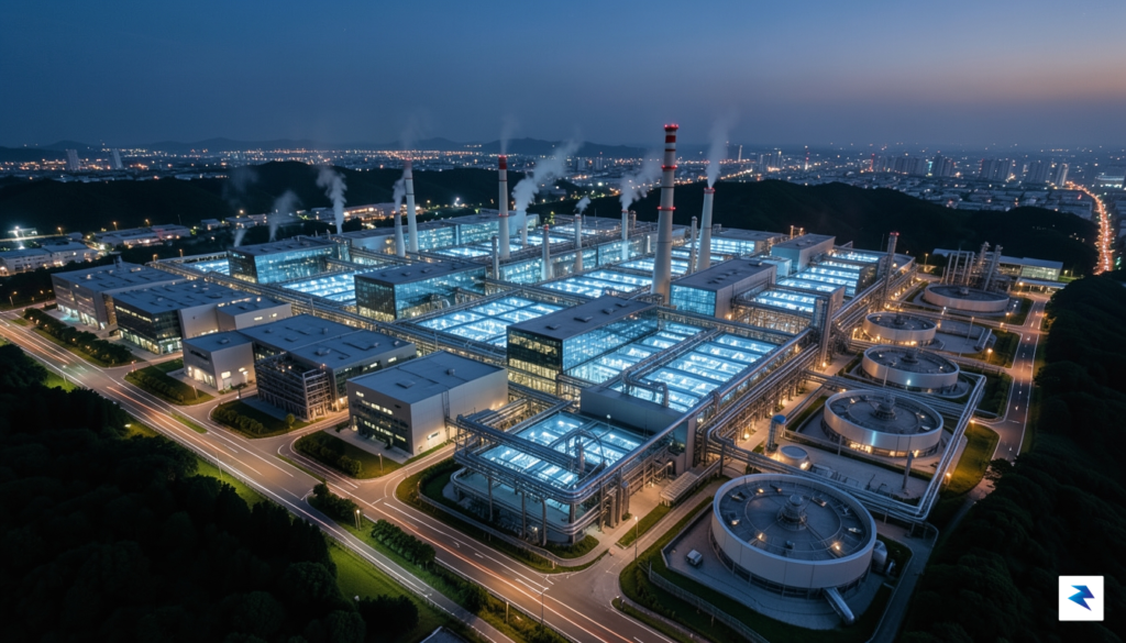
The sheer scale of South Korea’s $550 billion investment commitment represents a watershed moment for the global semiconductor landscape, effectively signaling a transition from incremental capacity growth to a wholesale industrial transformation. By funneling this unprecedented capital into new fabrication facilities and research infrastructure, the nation is actively insulating itself against the volatile supply chain disruptions that have come to be known as “RAMageddon.” This massive deployment of resources is not merely about increasing output; it is a calculated effort to fortify the entire semiconductor ecosystem against future geopolitical shocks while ensuring that the country remains the indispensable engine of the global digital economy.
At the center of this ambitious strategy are industry titans Samsung Electronics and SK Hynix, both of which are recalibrating their operations to meet the insatiable demands of the artificial intelligence era. Samsung is aggressively pivoting toward next-generation memory architectures and advanced packaging solutions that are essential for the high-bandwidth memory (HBM) chips required by modern AI models. Simultaneously, SK Hynix is leveraging its leadership in HBM technology to secure long-term partnerships with the world’s leading AI chip designers. Together, these companies are shifting their focus from being simple mass-market component manufacturers to becoming holistic partners in the AI value chain, providing the critical hardware foundation upon which generative AI and large language models are built.
The $550 billion investment is not just a financial figure; it is a statement of intent that South Korea will dictate the pace of the global AI revolution by controlling the essential silicon architecture of the future.
This massive capital expenditure is bolstered by a deeply symbiotic relationship between the private sector and the South Korean government, which has prioritized the semiconductor industry as a matter of national security. Policymakers are actively streamlining regulatory hurdles, providing tax incentives, and investing in specialized workforce development programs to ensure that these massive fabrication sites have the talent and stability needed to flourish. By aligning national economic policy with the long-term goals of these corporate giants, the government is creating a cohesive “semiconductor belt” that integrates research, development, and mass production into a singular, unstoppable engine. Through this strategic cooperation, South Korea is not only aiming to defend its current market share but is proactively architecting a future where it remains the primary gatekeeper of the world’s most advanced computing components.
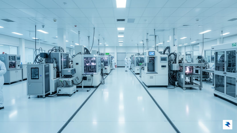
The AI Infrastructure Bottleneck

At the heart of the current artificial intelligence explosion lies a fundamental architectural paradox: while AI models are becoming exponentially more complex, the speed at which they can access and process information is increasingly constrained by the physical limitations of memory hardware. Modern graphical processing units (GPUs) are marvels of computational power, capable of performing trillions of operations per second, yet they are essentially rendered idle if they cannot receive data at a commensurate speed. This phenomenon, often described as the “memory wall,” occurs when the processor outpaces the memory’s ability to feed it information, leading to costly idle cycles that throttle the entire training pipeline. Consequently, the industry is shifting away from general-purpose DRAM toward High Bandwidth Memory (HBM3 and beyond), which functions as the critical lifeblood of machine learning.

Unlike traditional DRAM used in standard consumer computing, HBM3 chips utilize a 3D-stacked architecture, vertically connecting multiple memory dies with “through-silicon vias.” This design allows for a significantly wider communication bus, enabling massive amounts of data to be transferred between the memory and the processor simultaneously. For large language models and generative AI systems, this bandwidth is non-negotiable; without the rapid throughput provided by these specialized chips, the training of neural networks would take months longer than it currently does. As these models continue to scale in parameter count, the demand for memory density and speed has moved from a performance luxury to a structural necessity for any enterprise-grade AI infrastructure.
The transition to specialized memory is not merely an incremental upgrade; it is a complete reimagining of the hardware stack required to sustain the next decade of autonomous intelligence.
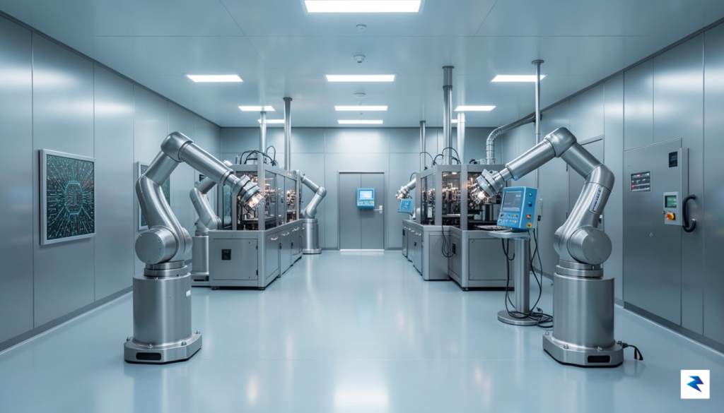
The manufacturing complexity associated with these advanced chips is immense, necessitating a massive expansion of fabrication capacity. Because HBM3 is so difficult to produce—requiring precision alignment and advanced thermal management—the global supply chain is currently in a state of high tension. South Korean tech giants are responding by funneling hundreds of billions of dollars into new, state-of-the-art fabs designed specifically for these high-performance memory modules. By prioritizing this infrastructure now, these companies are attempting to preempt a long-term bottleneck that could otherwise stall the global AI race. Investing in these massive manufacturing plants is, in essence, an insurance policy against the systemic throttling of the most powerful computing platforms ever created.
Global Semiconductor Supply Chain Repercussions

The staggering $550 billion infusion into South Korea’s semiconductor infrastructure is poised to act as a definitive counterweight to the volatility that has defined the memory market for years. By drastically expanding manufacturing capacity for high-bandwidth memory (HBM) and next-generation DRAM, firms like Samsung and SK Hynix are effectively signaling an end to the chronic shortages that have hampered global tech output. As this massive supply influx hits the market, economists anticipate a period of price stabilization that will provide much-needed relief for manufacturers of everything from consumer smartphones to high-end enterprise servers. This move is not merely about meeting current demand; it is a calculated effort to preemptively saturate the market, ensuring that the surging requirements of artificial intelligence and data center expansion do not trigger another catastrophic cycle of scarcity.
However, this immense concentration of production capacity within a single geographic region introduces a complex geopolitical paradox. While South Korea’s commitment guarantees a reliable pipeline for advanced memory chips, it simultaneously deepens the world’s reliance on a singular technological hub. In an era where supply chain resilience is synonymous with national security, having the majority of the world’s most advanced memory logic concentrated in the Korean Peninsula creates a significant single point of failure. Should regional instability or unforeseen logistical disruptions occur, the impact on the global digital economy would be instantaneous and severe, effectively leaving international markets vulnerable to a new form of systemic risk.

To mitigate these concerns, industry analysts and policymakers are increasingly emphasizing the necessity of a balanced approach that favors regional production diversity alongside this massive Korean investment. While the efficiency of South Korea’s existing “semiconductor cluster” is unmatched, the global market is pushing for a hybrid strategy: one where localized manufacturing hubs in the United States, Europe, and Japan operate in tandem with Korean production. This strategy aims to create a redundant, multi-layered supply chain that can withstand localized shocks without stalling global innovation.
The challenge for the next decade is not just building more capacity, but building the right kind of capacity that ensures equitable access and geographic security for critical technological components.
Ultimately, the $550 billion investment serves as both a solution and a catalyst for change. By front-loading the supply chain with such significant capacity, South Korea is securing its role as the backbone of the AI revolution, yet it also invites a global conversation about the risks of over-centralization. As the market digests this influx of production, the focus will undoubtedly shift toward how nations can harmonize their domestic tech ambitions with the reality of an inextricably linked, globalized semiconductor ecosystem. Successfully navigating this transition will determine whether the world achieves a stable, high-performance future or merely trades one form of supply chain volatility for another.
Future Outlook: Can Supply Meet Demand?


While the monumental $550 billion pledge from South Korea’s tech titans represents a foundational shift in global supply chain strategy, the transition from capital commitment to operational reality is a marathon, not a sprint. Constructing a state-of-the-art semiconductor fabrication plant—often referred to as a “fab”—is a multi-year endeavor that requires complex logistical coordination, environmental approvals, and the installation of ultra-precise lithography equipment. As these facilities slowly come online over the next decade, the industry faces a critical temporal mismatch: software-driven AI development evolves at an exponential pace, often iterating on a weekly or monthly basis, while hardware manufacturing remains tethered to the rigid, time-consuming physics of building physical infrastructure.
Bridging this gap requires more than just pouring concrete and ordering machinery; it demands sustained innovation in architecture and power efficiency. If the industry relies solely on sheer manufacturing scale to solve the bottleneck, it risks being perpetually one step behind the insatiable appetite of large language models and autonomous systems. Instead, the next ten years must prioritize the development of high-bandwidth memory (HBM) and specialized processing units that can do more with less. By focusing on modular chip designs and advanced packaging techniques, tech leaders can ensure that the chips produced in these new facilities remain relevant even as AI software requirements shift unpredictably throughout the late 2020s.
The true measure of this investment will not be the number of wafers produced, but the strategic reduction in the latency between architectural breakthroughs and mass-market deployment.
Looking toward 2030, this massive injection of capital is poised to permanently reshape the AI landscape. We are likely to see a transition from the current “scarcity mindset,” where access to compute power is a luxury, to an era of ubiquitous AI integration across everything from consumer electronics to industrial robotics. By the time these massive fabrication complexes reach full capacity, they will likely serve as the bedrock of a new global digital economy, effectively decoupling technological progress from the volatility of short-term supply chain disruptions. Ultimately, the success of this $550 billion bet hinges on the industry’s ability to synchronize its slow-moving hardware foundations with the rapid-fire evolution of the software world, ensuring that the hardware of tomorrow is ready to support the innovations we have yet to even imagine.