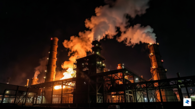
British Steel Nationalized: Why the U.K. Is Taking Control of Its Last Major Mill
The End of an Era: Understanding the British Steel Nationalization The decision to bring British Steel under state control represents far more…
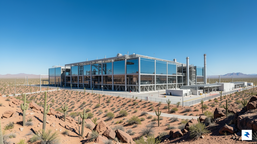
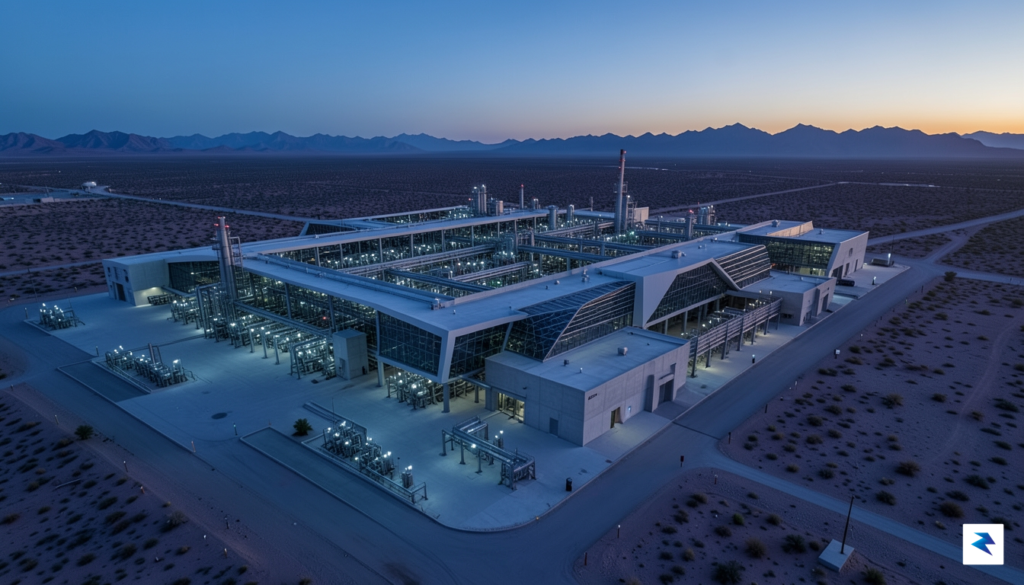
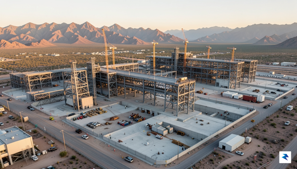
The transformation of Arizona into the bedrock of American semiconductor manufacturing did not happen by accident, but rather through a calculated alignment of geography, infrastructure, and policy. Phoenix and its surrounding suburbs, particularly the northern reaches of the valley, offered a rare combination of seismic stability, abundant land, and a pre-existing talent pool cultivated by decades of aerospace and legacy chip manufacturing. When TSMC first signaled its intent to establish a footprint in the U.S. back in 2020, the choice of Arizona was a clear signal that the company sought more than just a production site; it sought a permanent home that could function as a self-sustaining ecosystem for advanced logic manufacturing.
What began as a foundational $12 billion investment has since ballooned into a staggering $265 billion commitment, marking one of the largest foreign direct investments in American history. This escalation reflects a rapid shift in the global geopolitical climate, where the security of the semiconductor supply chain has transitioned from a business concern to a matter of national interest. As the facility plans expanded from a single fab to a complex network of interconnected plants, the synergy between TSMC and the local government became the blueprint for the modern American industrial renaissance. By integrating the project into the broader framework of the CHIPS and Science Act, the initiative successfully bridged the gap between private enterprise and federal incentives, ensuring that Arizona remains the critical nexus for the next generation of artificial intelligence and high-performance computing hardware.
The scale of this investment represents a fundamental shift in how the United States views its technological sovereignty, transforming the desert into the most vital node for advanced silicon production outside of Taiwan.
The success of this hub relies heavily on a symbiotic relationship that extends beyond mere capital infusion. Local utilities, educational institutions like Arizona State University, and state-level economic development agencies have worked in lockstep to provide the specialized water management, power grid capacity, and engineering pipelines required to keep these facilities running at peak efficiency. This evolution has effectively de-risked the prospect of domestic production, proving that even with significantly higher operating costs, the U.S. can compete by leveraging technological superiority and geographic stability. As the facility continues to grow, it serves as the ultimate proof point for the efficacy of current industrial policies, cementing Arizona’s reputation as the primary battleground where the future of global computing hardware is being forged.

The monumental expansion of TSMC’s footprint in Arizona to a staggering $265 billion represents far more than just the construction of industrial real estate; it is a fundamental restructuring of the global semiconductor supply chain. By layering this new $100 billion commitment atop existing plans, the company is effectively insulating the United States against the geopolitical volatility that has historically characterized chip production. This capital is not being funneled into singular, isolated facilities but is instead building a self-sustaining ecosystem where raw materials, sophisticated supply chains, and specialized labor pools converge. Consequently, the sheer scale of this investment ensures that the U.S. will host the most advanced manufacturing nodes currently available, effectively anchoring the next decade of American technological dominance.
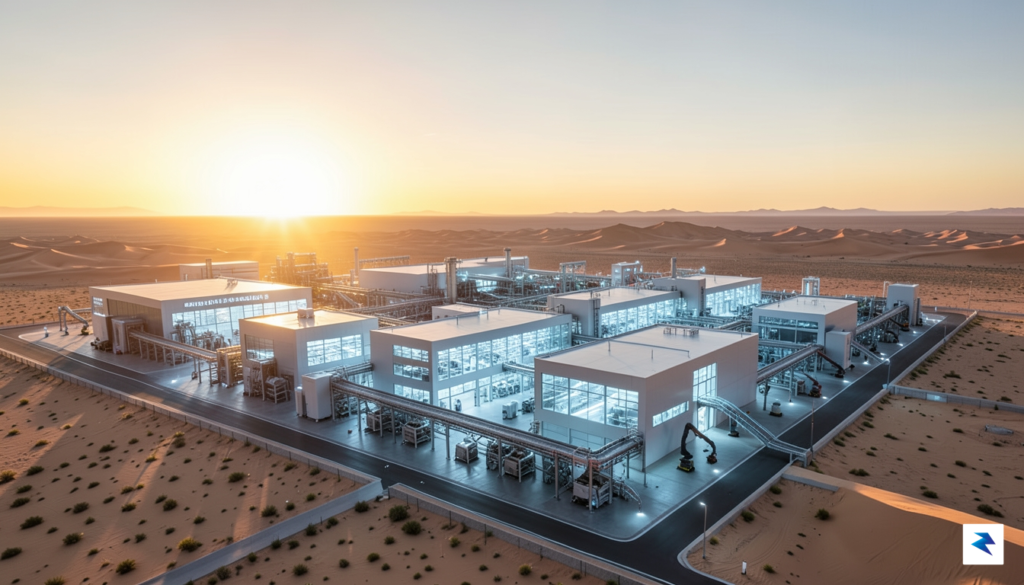
At the heart of this financial strategy lies a critical transition in manufacturing precision: the move from 5nm process technology to the cutting-edge 2nm node. While the initial investment phases focused on establishing a foothold with 5nm capabilities, this latest infusion of capital is explicitly earmarked for the infrastructure required to produce 2nm chips at scale. This transition is not merely an incremental improvement; it is a quantum leap in transistor density and energy efficiency. By producing 2nm semiconductors on U.S. soil, TSMC is bridging the gap between domestic manufacturing and the most advanced computing requirements of the modern era, ensuring that American firms do not have to rely on overseas foundries for their most sensitive and powerful hardware.
The leap to 2nm represents the frontier of physics in computing, where the ability to etch billions of transistors onto a sliver of silicon determines the winners of the global AI race.
Furthermore, this high-scale capital expenditure is the only viable response to the insatiable, AI-driven demand currently sweeping through the global market. Modern artificial intelligence models require immense computational power, necessitating chips that are both lightning-fast and incredibly power-efficient. Without this level of investment, the domestic manufacturing capacity would remain tethered to legacy technologies that cannot sustain the computational loads required for generative AI and real-time machine learning. By aggressively funding this expansion, TSMC is proactively aligning its manufacturing capacity with the future trajectory of the tech sector, ensuring that the necessary hardware backbone for artificial intelligence is built exactly where the demand is highest.

For decades, the global semiconductor industry has operated under a precarious paradox: while the world’s digital economy relies on advanced logic chips, the manufacturing of these components has remained heavily concentrated in Taiwan. This geographic bottleneck has long been viewed as a significant geopolitical vulnerability, as any disruption to the Taiwan Strait could potentially halt the production of everything from consumer smartphones to critical military hardware. By committing an additional $100 billion to its U.S.-based operations, TSMC is fundamentally altering this landscape, shifting from a model of centralized production to one of distributed, resilient infrastructure. This strategic pivot is not merely about capacity expansion; it is an insurance policy for the global tech ecosystem, ensuring that the most sophisticated silicon processors remain accessible even amidst escalating regional tensions in East Asia.

The concept of supply chain resiliency has moved from corporate buzzword to national security priority, and localized production is the ultimate answer to the fragility of global trade. By establishing leading-edge node manufacturing in Arizona, TSMC is drastically shortening the physical distance between the foundry and the end-user. This localization significantly mitigates the risks associated with oceanic shipping, such as port congestion, geopolitical blockades, and rising fuel costs, which have historically introduced unpredictable delays into the development cycle. When chips are manufactured closer to the design centers of Silicon Valley, the logistical feedback loop between chip designers and production engineers becomes faster and more efficient, creating a more agile manufacturing pipeline that can adapt to rapid market shifts.
The shift toward U.S. manufacturing represents a transition from “just-in-time” supply chains to “just-in-case” resilience, prioritizing availability and security over the lowest possible production costs.
For major domestic players like Apple, NVIDIA, and AMD, having local access to leading-edge nodes provides a distinct competitive advantage that transcends simple logistics. These industry titans require constant iteration and high-volume output to maintain their dominance in artificial intelligence and high-performance computing, sectors where even a week of downtime can be catastrophic. By embedding themselves within the U.S. manufacturing ecosystem, these companies can better safeguard their intellectual property and ensure a steady supply of hardware, regardless of international volatility. This domestic footprint effectively anchors the most critical segment of the tech supply chain on American soil, fostering an environment where innovation is shielded from the whims of cross-Pacific instability and regional conflicts.
Ultimately, this massive investment serves as a cornerstone for a new era of semiconductor autonomy. By diversifying production hubs, TSMC is helping to weave a more robust net that can withstand localized shocks, thereby stabilizing the global economy against future disruptions. As these facilities reach full capacity, the reliance on Taiwan will be supplemented by a powerful, high-tech engine in the American Southwest, signaling a profound realignment of the global chip market that benefits both the manufacturers and the nations that host them.
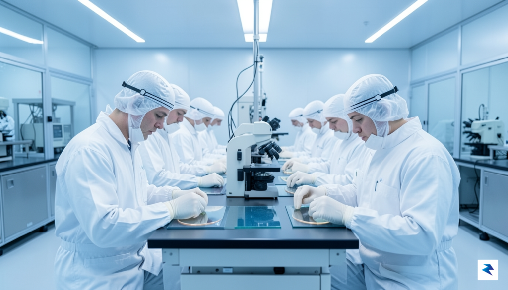
Beyond the headline-grabbing financial figures, the success of this monumental expansion rests on a complex foundation of logistical and human capital requirements. Transforming a patch of desert into a world-class semiconductor hub demands more than just capital; it requires a robust ecosystem of specialized infrastructure. TSMC’s operations are notoriously resource-intensive, necessitating an incredibly stable power grid and high-volume water reclamation systems capable of purifying and recycling millions of gallons daily. To meet these needs, the company has worked closely with local Arizona utility providers to fortify the regional energy infrastructure, ensuring that even a momentary flicker in power—which can ruin batches of microchips worth millions—is statistically improbable.
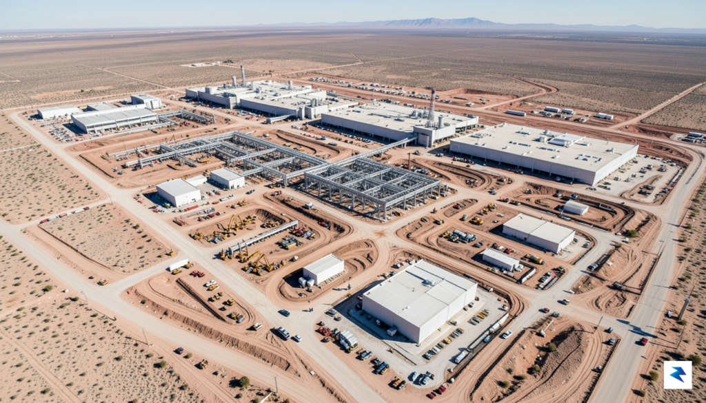
Perhaps the most daunting hurdle is the “talent gap.” Semiconductor manufacturing is an exacting discipline that requires thousands of highly trained technicians and engineers, a workforce that is currently in short supply within the United States. To bridge this divide, TSMC has forged strategic partnerships with Arizona State University and other regional educational institutions. These collaborative pipelines are designed to fast-track curriculum development, offering students hands-on apprenticeships that align academic theory with the high-stakes reality of a clean-room environment. By investing in these local training programs, the firm is attempting to create a sustainable, homegrown talent pool rather than relying exclusively on importing expertise from abroad.
The true test of this investment is not the speed of construction, but the long-term integration of a highly precise manufacturing culture into a new geographic and labor market.
Furthermore, the project represents a significant experiment in cross-cultural operational management. Integrating the legendary, high-intensity Taiwanese work culture—characterized by rapid iterative problem-solving and long hours—with American labor expectations and regulatory frameworks has presented a unique set of management challenges. Achieving harmony in this environment requires more than just translating technical manuals; it demands a fundamental rethinking of communication styles and labor relations. As management balances these divergent approaches, the goal is to create a hybrid workplace that maintains TSMC’s signature operational efficiency while respecting the professional norms of the local workforce. Successfully navigating this cultural synthesis will ultimately determine whether this Arizona endeavor becomes a blueprint for future global manufacturing or a cautionary tale of mismatched expectations.

The monumental expansion of TSMC’s footprint on American soil represents far more than a simple increase in manufacturing capacity; it signifies a structural pivot away from the fragile, hyper-centralized supply chains that have defined the tech industry for the last three decades. By internalizing the production of the world’s most advanced microchips, the United States is effectively mitigating the geopolitical risks associated with over-reliance on overseas foundries. This transition ensures that the backbone of modern innovation—from artificial intelligence algorithms and autonomous vehicle systems to critical defense infrastructure—remains anchored within domestic borders. As these facilities move from construction to full-scale operation, the nation is steadily insulating its technological progress from the volatility of global trade disruptions and international tensions.
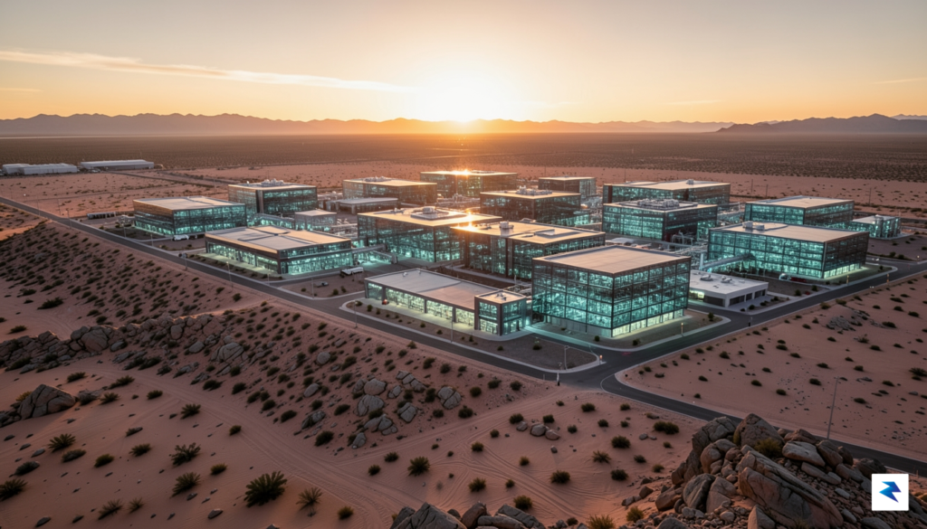
Beyond the immediate goal of national security, the localized economic impact of this multi-billion dollar investment is poised to create a massive multiplier effect across the Southwest. Arizona is rapidly evolving into a global hub for high-tech manufacturing, fostering an ecosystem that extends well beyond the fabrication plants themselves. This influx of capital is catalyzing the growth of a sophisticated supply chain, ranging from chemical and gas suppliers to specialized logistics providers and high-precision equipment maintenance firms. Furthermore, the demand for a highly skilled workforce is incentivizing unprecedented collaboration between academic institutions and private industry, ensuring that the next generation of American engineers is trained to lead in the fields of nanotechnology and semiconductor physics.
The long-term success of this initiative will be measured not just by the number of wafers produced, but by the resilience and intellectual capital it anchors within the U.S. economy for decades to come.
Looking toward the 2030 horizon, the global semiconductor landscape will look fundamentally different than it does today. As the United States regains its footing in front-end manufacturing, the global market is likely to shift toward a multi-polar model, where regional self-sufficiency becomes a standard competitive benchmark. While global trade in electronics will certainly remain robust, the concentration of critical “bleeding-edge” production capacity within American borders will provide the U.S. with a significant strategic advantage. By the end of this decade, this industrial pivot will likely be viewed as the catalyst for a new era of American technological dominance, characterized by a hardened supply chain, a revitalized domestic manufacturing sector, and the continued ability to drive the global frontiers of artificial intelligence and high-performance computing.
You must be logged in to post a comment.