
Why IMAX Is the Only Way to See Modern Blockbusters
The Immersive Scale of IMAX Cinema IMAX cinema is frequently misunderstood as merely a bigger screen, a simple upgrade in size for your…
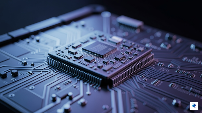

As artificial intelligence models continue their exponential growth in complexity and scale, the foundational hardware upon which they run has become an increasingly critical bottleneck. Traditional off-the-shelf processors, while powerful, often struggle to keep pace with the unique and demanding computational patterns inherent in modern AI workloads. This burgeoning gap between software ambition and hardware capability has prompted a fundamental shift among tech giants, particularly Google, towards a strategy of deep vertical integration, where the design of custom silicon becomes as crucial as the algorithms themselves.
Google’s journey into bespoke AI hardware is not a recent development; it began years ago with the pioneering introduction of the Tensor Processing Unit (TPU). Recognizing early on that general-purpose processors like CPUs and even GPUs were not optimally designed for the repetitive, matrix-heavy computations central to neural networks, Google embarked on creating application-specific integrated circuits (ASICs) tailored precisely for these tasks. Initially deployed to accelerate inference for services like Google Search and Street View, TPUs quickly evolved to handle demanding AI model training, demonstrating a clear commitment to specialized hardware long before the current AI boom.
This pivot from general-purpose GPUs to domain-specific architectures like the TPU highlights a critical insight: while GPUs excel at parallel processing across a wide array of computational problems, AI, and particularly deep learning, possesses distinct characteristics that allow for hyper-optimized hardware. These specialized chips can eliminate unnecessary general-purpose components, streamline data flow, and implement specific operations (like matrix multiplication) with unparalleled efficiency. The result is significantly improved performance per watt and per dollar, crucial metrics when operating AI at Google’s global scale, where even marginal gains translate into massive savings and capabilities.
The imperative for vertical integration has become even more pronounced with the advent of Large Language Models (LLMs) such as Google’s Gemini. These models are not just large; they are colossal, requiring unprecedented amounts of computational power, memory bandwidth, and intricate communication between thousands of accelerators. Relying solely on external hardware providers, no matter how advanced their offerings, introduces compromises. A generic chip, designed to serve a broad market, cannot be perfectly tuned to the specific nuances and architectural demands of Google’s proprietary LLMs and their training methodologies.
Therefore, developing custom AI chips specifically for Gemini allows Google to co-design the hardware and software stack in unison, unlocking efficiencies simply impossible with a disconnected approach. This bespoke engineering enables fine-grained control over every aspect, from the instruction set and memory hierarchy to the interconnects between chips within a data center. The ultimate goal is to drastically reduce the latency, increase the throughput, and lower the energy consumption associated with training and running these next-generation AI models, pushing the boundaries of what’s computationally feasible. This strategic move ensures that as AI continues to evolve, Google’s foundational infrastructure can evolve with it, offering a distinct advantage in the fiercely competitive AI landscape.

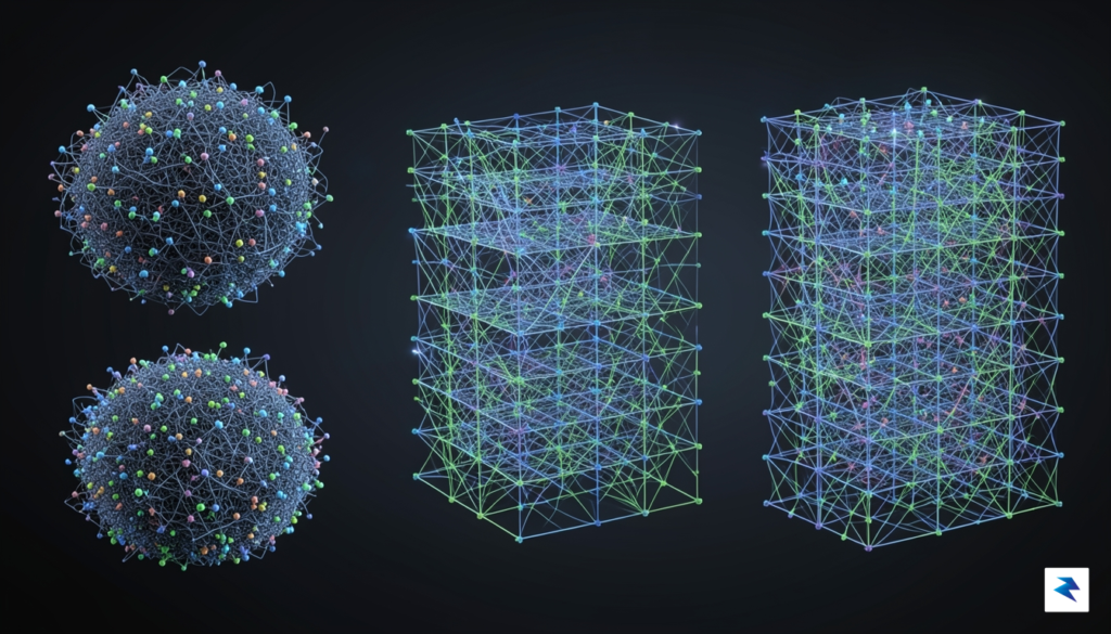
The computational demands placed upon modern artificial intelligence models, particularly advanced suites like Gemini, far exceed the capabilities of general-purpose computing hardware. Gemini is not merely a sophisticated chatbot that processes and generates text; it is a true multimodal powerhouse, capable of understanding and interacting with information across text, images, audio, and even video. This means that at any given moment, the model might be analyzing the nuances of a written prompt, interpreting the visual context of an uploaded image, deciphering spoken language, or understanding the temporal dynamics of a video clip. Handling these diverse data types concurrently, integrating them into a coherent understanding, and generating multimodal responses requires an astronomical amount of parallel processing and intricate data orchestration.
At the heart of Gemini’s operation lies the transformer architecture, a highly complex neural network design renowned for its effectiveness in language tasks but also incredibly resource-intensive. During inference – the process where the model generates an output based on an input – billions of parameters must be loaded, processed through multiple layers of attention mechanisms, and undergo vast matrix multiplications. Standard CPUs and even general-purpose GPUs, while powerful, often encounter significant bottlenecks when dealing with the sheer scale and specific computational patterns of these operations. The challenge isn’t just about raw computational FLOPs (floating-point operations per second); it’s about efficiently moving and manipulating colossal datasets of weights and activations with minimal latency.
The most critical bottlenecks often manifest in memory bandwidth and access patterns. Large language and multimodal models have billions, sometimes trillions, of parameters that need to be constantly accessed and updated from memory. If the speed at which the processing units can retrieve this data from dynamic random-access memory (DRAM) is slower than the speed at which they can compute, the system becomes “memory bound.” This “memory wall” leads to frustrating delays, where the powerful processing cores sit idle, waiting for data. Furthermore, the irregular memory access patterns inherent in transformer attention mechanisms can exacerbate this issue, preventing optimal utilization of memory caches and further slowing down the entire inference process.
This is precisely where specialized custom silicon, like the new AI chip Google is developing, becomes indispensable. These chips are engineered from the ground up to address the unique requirements of models like Gemini, moving beyond the general-purpose design of standard hardware. They integrate high-bandwidth memory (HBM) directly into the chip package, placing the data physically closer to the processing cores and dramatically increasing the speed and efficiency of data transfer. Moreover, custom instruction sets and optimized data flow architectures are designed specifically to accelerate the massive matrix multiplications and attention operations that dominate transformer model inference. By meticulously optimizing memory access patterns and ensuring data can flow seamlessly and rapidly to the computational units, these specialized chips can unlock significantly faster, more accurate, and substantially more energy-efficient performance for Gemini across all its complex multimodal tasks.
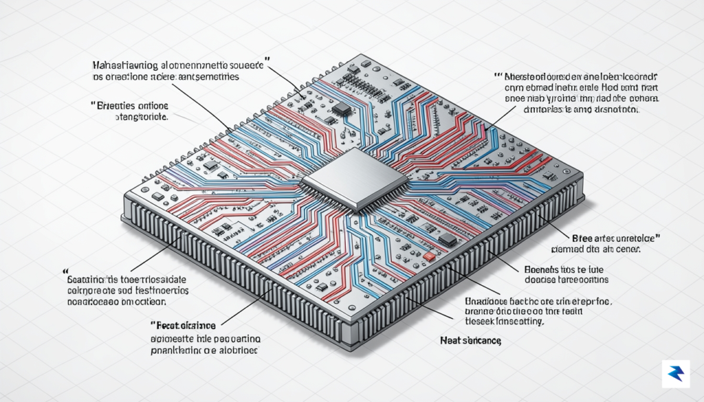
The burgeoning demands of sophisticated AI models like Gemini necessitate a new breed of hardware, and Google’s latest AI chip is poised to deliver just that. At its core, the architectural philosophy behind this new silicon is a relentless pursuit of efficiency: maximizing the computational throughput for complex AI tasks while simultaneously minimizing the energy expenditure per inference cycle. This dual focus is critical for scaling AI, whether powering advanced capabilities in data centers or enabling more intelligent experiences on personal devices. The expected technical advancements span several critical areas, each designed to push the boundaries of what’s possible in real-time AI processing.
A primary area of enhancement undoubtedly lies within the chip’s Neural Processing Unit (NPU) cores. These specialized accelerators are the workhorses of AI inference, designed to execute the mathematical operations fundamental to neural networks with unparalleled speed. We can anticipate a significant increase in the sheer number of NPU cores, allowing for massive parallelization of tasks. Furthermore, these cores are likely to feature refined instruction sets specifically optimized for common AI operations, such as matrix multiplications and convolutions, making them inherently more efficient. Improvements in on-chip interconnects and caching mechanisms will ensure that data can flow seamlessly and rapidly between these numerous cores, preventing bottlenecks and maintaining peak performance even under heavy loads.
Complementing the enhanced compute capabilities is a critical focus on memory architecture, particularly the integration of High-Bandwidth Memory (HBM). HBM stacks multiple memory dies vertically, connecting them with incredibly dense pathways to achieve vastly superior bandwidth compared to traditional DRAM. For large language models like Gemini, which often have billions of parameters, rapid access to these parameters and intermediate data is paramount. By integrating HBM directly onto the chip package, Google can drastically reduce data latency and increase the rate at which data is fed to the NPU cores, eliminating the “memory wall” that often limits the performance of AI accelerators. This tight integration ensures that the powerful NPU cores are never left waiting for data, operating at their maximum potential.
Another pivotal innovation expected to drive efficiency is the sophisticated use of reduced-precision arithmetic. Traditionally, AI models have relied on 32-bit floating-point (FP32) numbers for high accuracy, but these require significant computational resources and memory bandwidth. Modern AI chips are increasingly leveraging lower precision formats, such as 8-bit integers (INT8) or even 4-bit floating-point (FP4) numbers, for inference. The new Google chip will likely feature hardware accelerators specifically designed to perform calculations using these reduced precision formats without sacrificing the quality of the AI output. This technique, often paired with advanced quantization-aware training or post-training quantization methods, allows for substantial reductions in power consumption, faster computation, and lower memory footprint, all while maintaining the high accuracy required for complex AI tasks. It’s a delicate balance, but one that is absolutely essential for making powerful AI models like Gemini more accessible and sustainable.
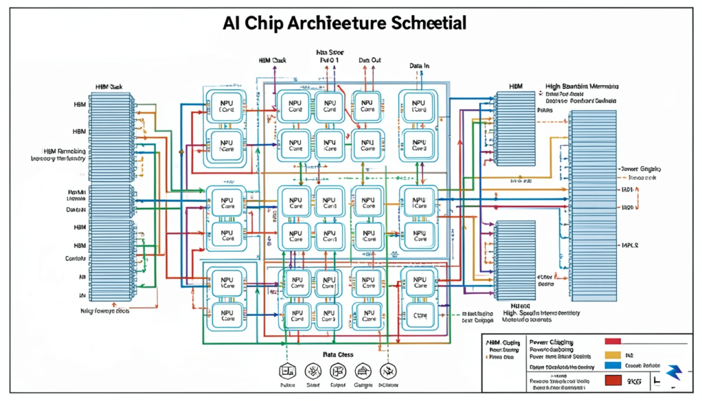
The synergy of enhanced NPU cores, tightly integrated HBM, and intelligent reduced-precision arithmetic forms the bedrock of an AI chip designed not just for speed, but for sustainable, energy-efficient intelligence at an unprecedented scale.
Collectively, these architectural improvements paint a picture of a chip meticulously engineered for the unique demands of next-generation AI. The focus on maximizing throughput and minimizing energy cost per inference cycle means that Gemini can operate with greater speed, handle more complex queries, and process larger datasets more efficiently than ever before. This foundational hardware innovation is crucial for unlocking new capabilities in AI, from more nuanced language understanding to faster, more robust generative models, ultimately shaping the future of intelligent computing.

The proliferation of advanced artificial intelligence models, particularly large language models (LLMs) like Gemini, has brought about unprecedented computational demands. Training and running these sophisticated neural networks at scale requires an immense amount of processing power, primarily housed within vast data centers globally. These facilities are veritable energy behemoths, consuming staggering quantities of electricity not just for the processors themselves, but also for the extensive cooling systems necessary to prevent overheating. Indeed, the energy footprint of modern data centers can often rival that of small cities or even entire nations, requiring massive infrastructure and contributing significantly to global carbon emissions and raising serious concerns about the long-term environmental sustainability of our increasingly AI-driven world. This escalating energy demand presents a critical challenge that necessitates innovative solutions.
In response to this pressing challenge, Google’s development of a new AI chip specifically optimized for its Gemini models represents a pivotal stride towards mitigating AI’s environmental impact. Unlike general-purpose computing hardware, which must cater to a wide array of tasks, a custom-designed AI accelerator can be meticulously engineered to perform the specific calculations central to LLM operations with far greater efficiency. This specialization means that the chip can execute complex AI inferences and potentially even training tasks using significantly less power per operation compared to off-the-shelf components. By tailoring the architecture, memory access patterns, and even the type of transistors used, these specialized chips can achieve a higher computational output for every watt of electricity consumed, thereby dramatically lowering the total power draw required to run Google’s AI services at their current, vast scale. This hardware-level optimization directly translates into a reduced carbon footprint, moving beyond software tweaks to address the fundamental energy cost of AI at its very core.
The implications of such hardware-level efficiency extend far beyond immediate energy savings; they lay the groundwork for a more sustainable future for AI itself. As artificial intelligence continues its rapid evolution, becoming ever more integral to various industries and daily life, the demand for computational resources will only escalate. Without significant advancements in energy efficiency, the environmental cost of scaling AI could become prohibitive, hindering innovation and widespread adoption. By drastically reducing the power requirements per computation, Google’s specialized chip enables the company to expand its AI capabilities and deploy more sophisticated models without a proportional increase in energy consumption, a critical factor as AI becomes more pervasive. This approach ensures that the growth of powerful AI, exemplified by Gemini, can proceed on a trajectory that is not only technologically ambitious but also environmentally responsible, making advanced AI services more accessible and sustainable for the long haul. Ultimately, this represents a crucial step towards decoupling AI’s incredible potential from its historically heavy energy burden.

Google’s strategic decision to develop its own artificial intelligence chip, specifically engineered to enhance the efficiency of its Gemini models, sends an unequivocal signal across the tech industry: future AI supremacy will hinge on comprehensive control over both the software algorithms and the underlying physical silicon. This move is far more than an engineering endeavor; it represents a profound realignment of market strategy, positioning Google to secure an enduring competitive advantage in the rapidly evolving AI landscape. By bringing chip design in-house, Google aims to tightly integrate its AI models with purpose-built hardware, unlocking unparalleled performance and efficiency gains that general-purpose solutions simply cannot match. It’s a bold declaration that true innovation in AI demands mastery from the foundational hardware layer all the way up to sophisticated applications.
This strategy directly contrasts with the established model championed by industry giants like NVIDIA, who have built a formidable ecosystem around their powerful GPUs and the ubiquitous CUDA software platform. NVIDIA’s strength lies in providing highly versatile, cutting-edge hardware that serves a broad spectrum of AI developers and cloud providers, acting as a crucial enabler across the entire industry. Google, however, is now pursuing a more vertically integrated path, opting to design silicon precisely tuned to the unique demands of its own Gemini architecture rather than relying on more generalized hardware solutions. This bespoke approach promises to deliver efficiencies and performance optimizations that are simply unattainable when adapting software to off-the-shelf components, giving Google a potential edge in specific, high-stakes AI applications.
The implications for third-party supplier dependency are substantial. Currently, many large AI developers, including Google to some extent, rely heavily on external chip manufacturers for the high-performance processors essential for training and deploying complex AI models. By developing its own chip, Google significantly reduces its reliance on these external suppliers, mitigating potential supply chain vulnerabilities and gaining greater control over its technological destiny. This newfound independence allows Google to dictate its own design cycles, integrate specific features tailored for Gemini, and optimize manufacturing processes, ensuring a more resilient and agile development pathway for its flagship AI initiatives. It’s about securing a strategic asset that is critical to its long-term growth and innovation trajectory.
Economically, owning the full AI stack presents compelling advantages. Firstly, it offers the potential for significant cost reductions, as Google can bypass the substantial markups typically associated with acquiring high-performance chips from third-party vendors. Furthermore, the ability to custom-design hardware means optimizing for energy efficiency and operational costs, a critical factor given the immense computational power required by modern AI models. Beyond direct financial savings, this vertical integration accelerates innovation by
You must be logged in to post a comment.