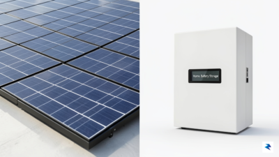
Is Solar Still Worth It? Navigating the New Economics of Home Energy
The Shifting Landscape of Residential Solar Economics For the past decade, the financial argument for going solar was remarkably…

For more than half a century, the steady cadence of Moore’s Law—the observation that the number of transistors on a microchip doubles roughly every two years—has dictated the pace of human innovation. This relentless scaling enabled the evolution from room-sized mainframes to the powerful smartphones currently sitting in our pockets. However, we have reached a precarious juncture where the physics of silicon are beginning to defy our ambitions. As we cram billions of transistors into spaces smaller than a biological cell, we are no longer merely facing engineering hurdles; we are bumping against the fundamental laws of thermodynamics and quantum mechanics.
The primary antagonist in this technological drama is heat. When transistors shrink to the scale of mere nanometers, the movement of electrons through copper wiring encounters significant resistance, which translates directly into thermal energy. This is not just a minor inconvenience; it is a physical barrier known as thermal throttling. When processors generate more heat than they can effectively dissipate, they are forced to slow down to prevent permanent damage to their internal architecture. Consequently, the power efficiency gains that once defined each new generation of hardware are evaporating, leaving us with chips that require increasingly complex cooling solutions just to maintain baseline performance.
Beyond the thermal crisis, we are also encountering the stubborn reality of signal latency. In a traditional electronic chip, data travels as electrical pulses through metallic interconnects. As these pathways grow narrower and more densely packed, the time it takes for a signal to traverse the chip—and the energy lost during that transit—becomes a major bottleneck. Even if we could theoretically print smaller transistors, the speed of electricity itself is not sufficient to satisfy the insatiable data demands of modern artificial intelligence and high-speed computing. The electrons, while fast, are hampered by the resistive properties of the very wires meant to guide them.
The reliance on electron-based signaling is shifting from an enabler of performance to a primary constraint on growth, signaling that the era of simple miniaturization has effectively reached its natural conclusion.
This diminishing return on scaling means that simply adding more transistors is no longer a viable path forward for the tech industry. We are essentially trying to squeeze more water through a pipe that is already at capacity; increasing the pressure only results in leaks and heat. To move past this stagnation, the industry must pivot away from the limitations of electron movement and explore fundamentally different paradigms of computing. By shifting the focus toward light-based signaling—where data is transmitted via photons rather than electrons—we may finally find the leverage needed to break free from the constraints of the silicon age and usher in a new epoch of computational speed.
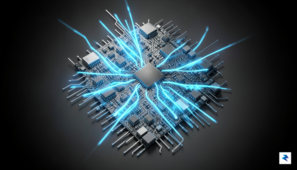
For decades, the microprocessing industry has relied on electrons moving through copper wires to shuttle data across a chip. While this approach served the early era of computing well, we have hit a physical wall where the resistance and heat generated by moving electrons threaten to stall further progress. As current increases, copper wires encounter electrical impedance, a phenomenon that slows down signal transmission and wastes significant energy as heat. This creates a bottleneck in modern AI-driven architectures, where the sheer volume of data moving between processors and memory requires a paradigm shift in how information is transported.
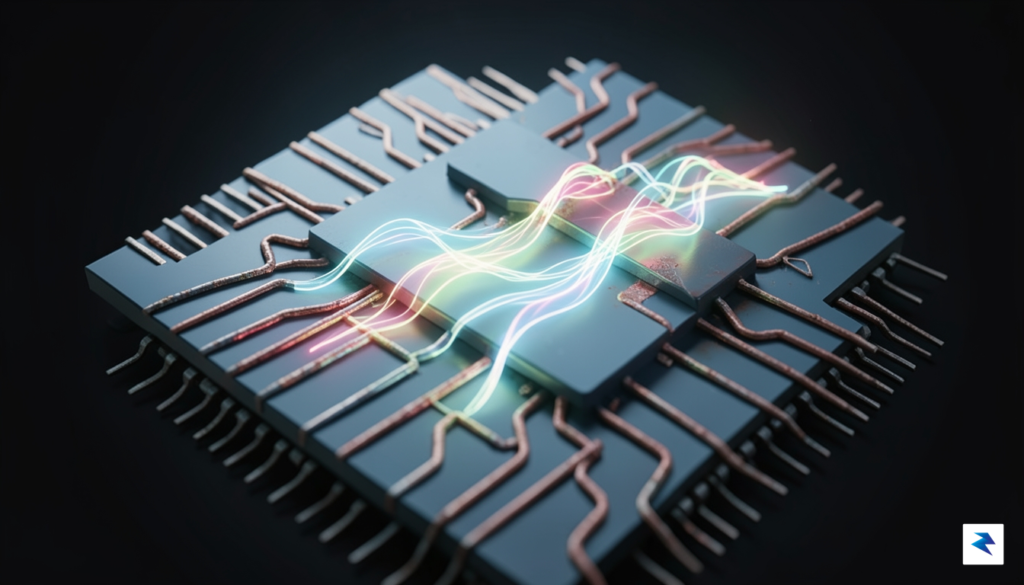
The solution lies in the promise of silicon photonics, a technology that swaps sluggish electrons for the near-instantaneous speed of photons. By integrating lasers directly onto the silicon substrate, engineers can transmit data as light pulses, which are immune to the electromagnetic interference and resistive heating that plague traditional metal interconnects. Because photons do not carry an electrical charge, they can move through optical waveguides with virtually no energy loss, allowing for a massive increase in bandwidth that far exceeds what is possible with conventional circuitry. This transition effectively removes the thermal ceiling that has hindered the scaling of high-performance computing.
The leap from electrical to optical signaling is comparable to moving from a crowded, narrow road to a high-speed fiber-optic highway; it is not just an incremental improvement, but a fundamental change in the physics of data movement.
Beyond the raw speed, the efficiency gains are transformative for the next generation of data centers and artificial intelligence hardware. When data moves via light, the energy required to transmit each bit drops precipitously, allowing for denser chip designs that don’t require the massive cooling infrastructure currently needed to keep supercomputers from overheating. By leveraging existing silicon manufacturing processes, the industry is now poised to integrate these optical components directly into the chips themselves, turning the processor into an engine of light. This integration represents the most viable path forward to extend the spirit of Moore’s Law, ensuring that as our appetite for computational power grows, our hardware is physically equipped to meet the demand.

For decades, the engine of computing progress was defined by how many transistors we could cram onto a sliver of silicon. However, as we enter the era of massive AI models, the primary constraint has shifted from how fast a chip can calculate to how quickly it can move data. Modern AI processors are incredibly powerful, yet they are increasingly held back by the limitations of traditional copper wiring. These metallic pathways, which serve as the central nervous system for data transport, are struggling to keep up with the sheer volume of information generated by massive training workloads. As the chips become faster, the traditional bus architectures act like a narrow country road trying to accommodate the traffic of a ten-lane superhighway, leading to a debilitating “interconnect bottleneck.”
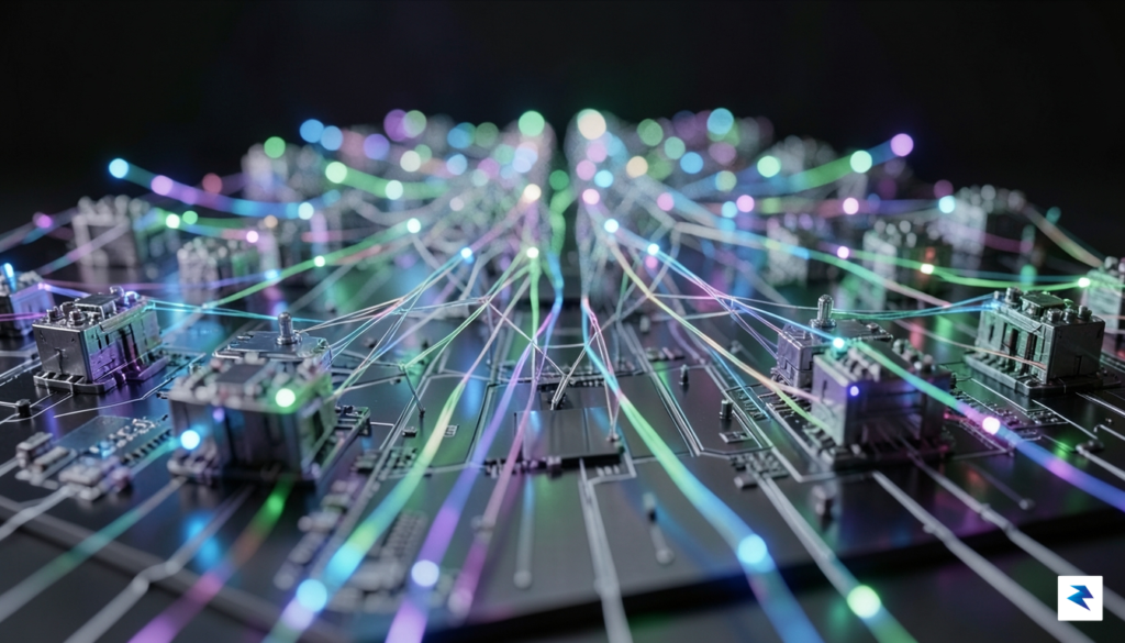
The energy cost of this inefficiency is staggering. In large-scale AI training, a significant portion of the total power consumption is not spent on actual computation, but rather on the physical movement of data across these copper interconnects. When electrons are forced through metal, they generate heat due to electrical resistance, a phenomenon that forces engineers to balance performance against thermal thresholds. If a chip spends more energy moving data than processing it, the entire system becomes inherently inefficient and difficult to scale. This is precisely why Pat Gelsinger and other industry leaders are looking toward silicon photonics as a definitive solution to this energy crisis.
The future of high-performance computing depends on replacing the sluggish flow of electrons with the near-instantaneous speed of photons.
By integrating optical bridges directly onto the chip architecture, engineers can move information using light instead of electricity. Because photons do not experience resistance in the same way that electrons do, they can carry vastly more data over longer distances without generating the same level of heat. This transition effectively removes the electronic “traffic jam” that has plagued hardware design for years. By allowing different components of an AI system to communicate at the speed of light, manufacturers can create more cohesive and powerful architectures that are no longer tethered to the physical limitations of copper. This shift is not just an incremental improvement; it is a fundamental redesign of how we define the speed and capacity of our most advanced computational engines.
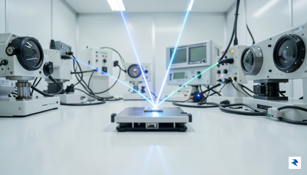
Transitioning from traditional copper-based interconnects to light-based data transmission is not merely an architectural shift; it represents a fundamental upheaval in how we conceptualize the semiconductor manufacturing lifecycle. For decades, the industry has relied on electrons moving through microscopic metallic pathways, but as we push toward the physical limits of miniaturization, heat dissipation and signal latency have become insurmountable roadblocks. Intel’s strategy centers on silicon photonics—a bold attempt to marry the speed of light with the sheer scale and cost-efficiency of existing silicon wafer fabrication. By leveraging their massive, globally distributed manufacturing infrastructure, the company aims to move beyond the experimental laboratory stage and into the realm of mass-market production, turning optical communication into a standard feature rather than an exotic luxury.
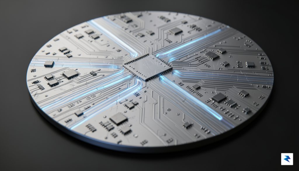
The primary technical hurdle in this transition is the integration of laser sources directly onto the silicon substrate. Historically, light-based components were bulky, discrete devices that were difficult to align with the precision required for high-volume chip manufacturing. Intel’s approach focuses on “heterogeneous integration,” a sophisticated process that bonds specialized materials—such as Indium Phosphide, which is ideal for generating light—directly onto silicon wafers. This allows them to create high-performance lasers that can be manufactured using standard, automated tools. The alignment challenges here are astronomical; because light must be coupled into tiny waveguides with sub-micron accuracy, any slight deviation during the manufacturing process can render the entire chip useless. Intel’s mastery of advanced packaging and lithography is the “secret sauce” that allows them to perform this delicate assembly at a scale that competitors simply cannot replicate.
The true breakthrough lies in the ability to treat optical components with the same high-volume, low-cost manufacturing discipline that has defined the silicon era for the last fifty years.
Beyond the lasers themselves, Intel must also perfect the integration of photodetectors and modulators that convert electrical signals into light and back again. Managing the thermal profile of these components is vital, as light-emitting materials are notoriously sensitive to temperature fluctuations. By embedding these optical engines directly into the chip package, Intel minimizes the distance data needs to travel, effectively slashing energy consumption while exponentially increasing bandwidth. This vertical integration—from the laser material science to the final assembly—is what positions the company to redefine the limitations of Moore’s Law. Ultimately, Intel is not just building a new type of chip; they are constructing a new foundation for the data-intensive future of artificial intelligence, where light becomes the primary language of the processor.

The advent of light-based computing promises a profound recalibration of our technological landscape, particularly within the burgeoning field of artificial intelligence. Today’s most sophisticated AI models, especially the large language models driving generative AI, are voracious consumers of computational power and energy, often limited by the electrical signaling bottlenecks inherent in traditional silicon chips. By leveraging photons instead of electrons for data transfer, these innovative photonic-enabled chips drastically increase bandwidth while simultaneously reducing power consumption, effectively unlocking a new frontier for AI development. This fundamental shift allows for the creation and deployment of far more complex and efficient generative AI models, making cutting-edge capabilities not only more powerful but also significantly more accessible to a broader range of applications and users.
Crucially, the implications for energy sustainability are monumental. The training and operation of current large-scale AI models contribute a growing and considerable carbon footprint, with massive data centers consuming staggering amounts of electricity for processing and cooling. Photonic chips, by their very nature, generate less heat and require substantially less power for data transmission compared to their electronic counterparts. This reduction in energy demand could lead to a dramatic decrease in the operational costs and environmental impact of AI infrastructure, offering a tangible path towards a more sustainable future for artificial intelligence and mitigating the energy crisis often associated with its rapid expansion.
Furthermore, this technological leap revitalizes the spirit of Moore’s Law, adapting its relevance for an era defined by machine learning rather than solely raw clock speed. While traditional electronic chips have been hitting physical limits in terms of transistor density and speed, the bottleneck for AI performance increasingly lies in the efficient movement of vast amounts of data between processing units and memory, and the power required to do so. Photonic interconnects and processing units circumvent these electrical limitations, enabling an exponential increase in effective compute capacity and data throughput. This not only allows for continuous performance improvements in AI hardware but also democratizes access to high-performance computing, fostering innovation across diverse industries worldwide.
While the full-scale adoption of photonic chips is not an overnight prospect, significant research and development are propelling this technology forward, suggesting a transformative impact within the next decade. As these light-driven components become more integrated into our computing infrastructure, we can anticipate a future where AI agents are not only more intelligent and responsive but also far more energy-efficient and scalable. This shift will enable the deployment of AI in novel ways and at unprecedented scales, from hyper-personalized digital assistants to complex scientific simulations, fundamentally reshaping how we interact with technology and solve global challenges.
You must be logged in to post a comment.