Why Bitcoin’s Sharpe Ratio is Hitting 2022 Lows: What Investors Need to Know
Understanding the Sharpe Ratio in Crypto At its core, the Sharpe ratio is the financial industry’s standard way of measuring the quality of an…

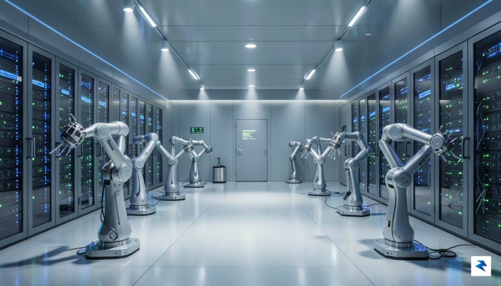
The exponential growth of generative artificial intelligence has fundamentally reshaped the technological landscape, shifting the focus from software innovation alone to the underlying physical infrastructure that powers these complex systems. Where once memory chips were largely considered commodity components, essential but undifferentiated, primarily serving consumer electronics like smartphones and personal computers, they have now ascended to the status of critical AI infrastructure. This profound transformation is driven by the insatiable demand for processing massive datasets and executing intricate neural network computations, tasks that quickly become bottlenecked by traditional memory’s limited bandwidth and capacity. Consequently, the performance of an AI system is no longer solely dictated by its central processing unit (CPU) or graphics processing unit (GPU), but equally by the speed and efficiency with which data can be moved to and from these powerful processors, making high-performance memory an indispensable core component.
Recognizing this seismic shift early on, SK Hynix, a long-standing titan in the semiconductor industry, embarked on a strategic pivot over the past three years that has profoundly redefined its market position. Instead of solely competing in the increasingly commoditized traditional DRAM market, the company made a prescient bet on High Bandwidth Memory (HBM), a specialized form of memory designed specifically for the rigorous demands of AI and high-performance computing. This forward-looking approach involved significant investment in research, development, and manufacturing capabilities to perfect HBM technology, which stacks multiple memory dies vertically to achieve unparalleled data transfer rates and energy efficiency. By focusing intently on these cutting-edge solutions, SK Hynix positioned itself not just as a memory supplier, but as an enabler of the most advanced AI accelerators, effectively securing its place at the very heart of the burgeoning AI hardware ecosystem.
This strategic foresight has directly intertwined SK Hynix’s fortunes with the meteoric rise of companies like Nvidia, the undisputed leader in AI GPU technology. Nvidia’s groundbreaking AI accelerators, such as the highly sought-after H100 and GH200 chips, owe much of their unparalleled performance to the integrated High Bandwidth Memory supplied by SK Hynix. These GPUs, engineered to handle the immense parallel processing loads of large language models and other AI workloads, require memory that can feed data to their thousands of cores at extraordinary speeds, a requirement perfectly met by HBM. SK Hynix has emerged as a primary, and often exclusive, supplier of the latest generations of HBM, making it an indispensable partner in Nvidia’s supply chain and, by extension, to the entire AI industry. This symbiotic relationship underscores how SK Hynix’s specialized memory solutions are not just components, but foundational pillars enabling the revolutionary capabilities of today’s most powerful artificial intelligence systems.
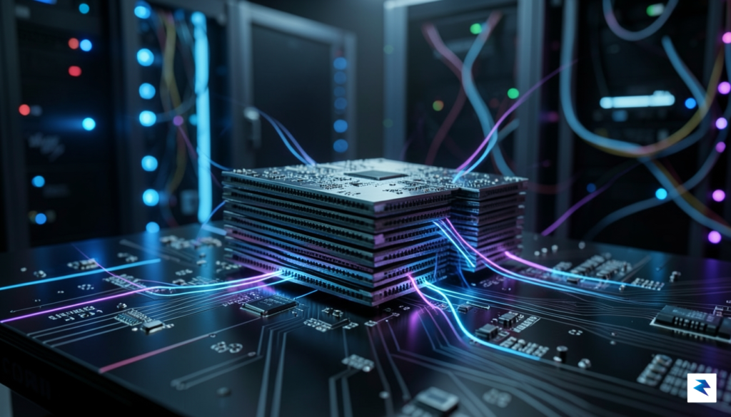
To understand why the artificial intelligence landscape is so fiercely competitive, one must first look at the physical limitations of modern computing. Traditional DRAM, the standard memory found in personal computers and servers for decades, is designed for general-purpose tasks where data access is relatively sporadic. However, training large language models (LLMs) requires moving gargantuan amounts of information between a processor and its memory banks thousands of times per second. When the memory cannot keep up with the processing speed of a GPU, the entire system experiences a “memory wall,” effectively idling expensive silicon while it waits for data to arrive. High-Bandwidth Memory (HBM) solves this by vertically stacking DRAM dies and connecting them via Through-Silicon Vias (TSVs), creating a multi-lane highway for data that is vastly wider and more efficient than traditional side-by-side memory configurations.
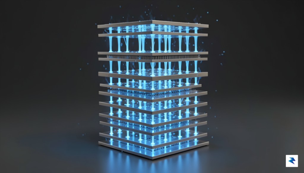
The technical superiority of HBM lies in its ability to deliver massive throughput while consuming significantly less power than traditional memory modules. By placing the memory physically closer to the GPU and utilizing a wider interface, HBM minimizes the latency that typically plagues AI training workloads. Because AI models like GPT-4 require billions of parameters to be read and updated in real-time, the energy efficiency of this architecture is just as critical as its speed. If a memory chip runs too hot or draws too much power, it creates a thermal bottleneck that forces the system to throttle performance, ultimately slowing down the training process and increasing operational costs for data centers.
The race for AI dominance is currently being won in the cleanrooms of semiconductor factories, where the ability to manufacture dense, high-yield stacks of HBM is the single most important indicator of a company’s long-term competitive moat.
SK Hynix has successfully established itself as the frontrunner in this niche, outpacing competitors like Samsung and Micron through superior production yields and aggressive innovation cycles. While other manufacturers have struggled with the complex thermal management and alignment precision required to stack these memory layers without defects, SK Hynix has refined its packaging technology to produce reliable, high-capacity HBM3 and HBM3E modules at scale. This execution advantage has made them the primary supplier for industry giants like NVIDIA, effectively positioning them as the backbone of the current AI infrastructure. For investors, this technical lead is not just a marketing claim; it represents a significant barrier to entry that competitors will find difficult to bridge, as the complexity of HBM manufacturing only increases with each new generation of chips.

The impending multibillion-dollar U.S. listing of SK Hynix represents a watershed moment for the global investor community, effectively dismantling the geographical barriers that have long sidelined American retail and institutional participation. For years, investors seeking exposure to the high-bandwidth memory (HBM) sector were forced to navigate complex international exchanges or settle for indirect, diluted exposure through broader semiconductor ETFs. By establishing a direct route to the U.S. capital markets, the company is not merely seeking a broader investor base; it is positioning itself as a central pillar of the Western AI infrastructure ecosystem. This transition toward greater transparency and accessibility effectively invites domestic portfolios to take a front-row seat in the ongoing AI memory gold rush, which has become the silent engine behind the current generation of generative AI models.
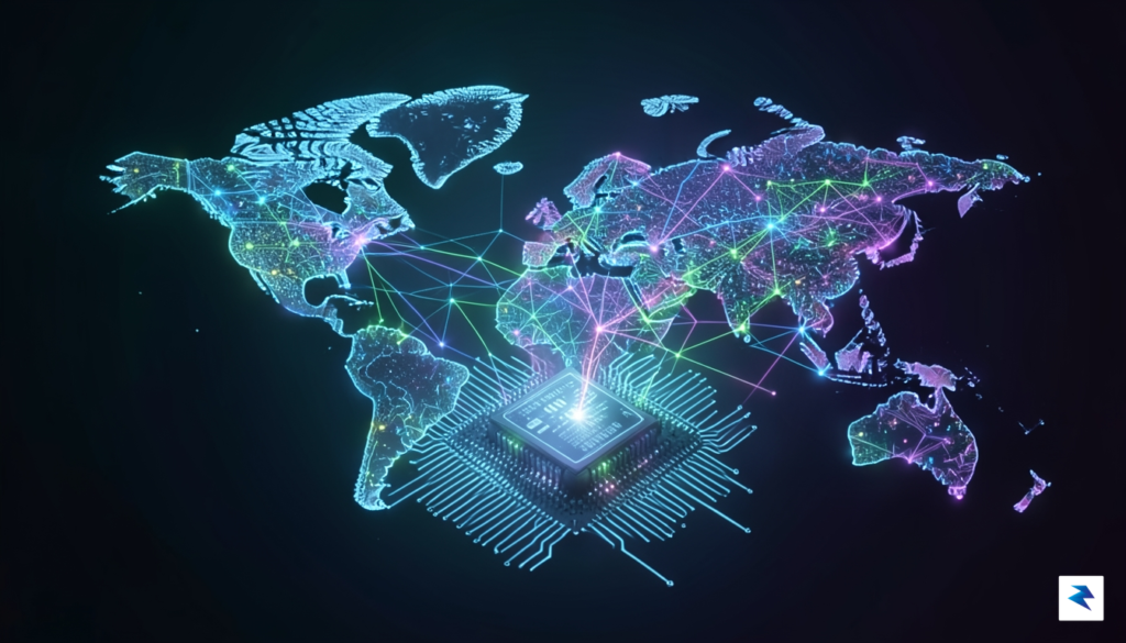
From a strategic standpoint, a U.S. IPO is a calculated maneuver designed to deepen stock liquidity and attract institutional heavyweights who demand the regulatory rigor of American exchanges. When a company of this magnitude lists on a major U.S. board, it undergoes a transformation in how it is perceived by global analysts, moving from a regional powerhouse to a globally integrated tech titan. Increased liquidity not only facilitates smoother entry and exit points for large-scale funds but also forces a higher level of corporate governance and financial disclosure. This creates a virtuous cycle where improved visibility attracts deeper capital, which in turn fuels the massive, multi-year expansion projects required to keep pace with the insatiable demand for AI-ready hardware.
The shift toward a U.S. listing serves as a powerful signal that the company is aligning its long-term financial trajectory with the epicenter of the global AI boom, ensuring that its capital-intensive expansion plans are backed by the world’s most liquid financial markets.
Furthermore, this listing mirrors a broader, tectonic shift among major chip manufacturers who are increasingly seeking to localize their capital structures alongside their physical manufacturing footprints. As SK Hynix invests heavily in state-of-the-art production facilities across the United States, a domestic IPO serves as a natural financial extension of that physical commitment. By syncing its ownership base with its operational geography, the company reduces currency risk and fosters a more cohesive relationship with its primary customers and regulatory partners. For the average investor, this convergence offers a rare opportunity to participate in the capital-intensive world of semiconductor manufacturing, providing a tangible stake in the foundational components that will define the next decade of computing.
While the explosive demand for high-bandwidth memory (HBM) is currently fueling a historic rally for semiconductor giants, prospective investors must look beyond the present AI euphoria to understand the industry’s notoriously volatile DNA. Historically, the memory sector has been defined by extreme “boom-and-bust” cycles, where periods of massive capital expenditure and supply shortages inevitably give way to gluts that decimate profit margins. Unlike software firms that scale with minimal marginal cost, memory manufacturers are tethered to the physical constraints of massive fabrication plants, which require billions in upfront investment. When supply catches up to demand, prices for standard DRAM and NAND chips can plummet overnight, forcing companies into intense price wars that test even the most resilient balance sheets.
Beyond the inherent cyclicality of the chip market, investors face a multifaceted landscape of external risks that could dampen the current AI-driven growth trajectory. Geopolitical tensions remain a significant wild card, particularly as memory manufacturing relies on complex, globalized supply chains that are increasingly vulnerable to trade restrictions and regional instability. Furthermore, fluctuating raw material costs—ranging from rare gases to specialized chemical precursors—can squeeze operating margins even when demand remains high. There is also the lingering concern of a potential “softening” in the AI hardware market; if enterprise spending on data center infrastructure hits a plateau, the current supply-demand imbalance could shift rapidly toward a surplus, leaving manufacturers with expensive, underutilized capacity.
To evaluate the long-term viability of a memory-focused company, investors should look past quarterly revenue spikes and prioritize metrics like R&D efficiency, capital allocation discipline, and the ability to maintain market share in premium, high-margin segments like specialized AI memory.
To navigate these turbulent waters, it is essential to adopt a framework that focuses on the company’s structural competitive advantages rather than just short-term earnings growth. A resilient memory manufacturer is typically one that has successfully diversified its product mix, moving away from commodity chips toward proprietary, high-value solutions that are “sticky” within the AI ecosystem. When assessing value, pay close attention to debt levels and free cash flow generation, as these are the primary buffers against the inevitable down-cycles of the semiconductor industry. By focusing on firms that demonstrate disciplined capital expenditure and technological leadership in HBM, investors can better position themselves to capture the rewards of the AI boom while mitigating the risks posed by the sector’s historical volatility.

The current surge in demand for High Bandwidth Memory (HBM) has positioned SK Hynix at the epicenter of the artificial intelligence revolution, but the true test lies in the company’s ability to transition from a rapid-growth phase to long-term architectural dominance. To maintain this momentum, the company has aggressively funneled capital into an R&D roadmap that prioritizes iterative leaps in memory density and energy efficiency. By focusing on next-generation HBM architectures—such as the transition toward HBM4 and beyond—SK Hynix is not merely reacting to market fluctuations; it is actively defining the hardware constraints that will dictate the performance limits of future large language models and autonomous computing systems.
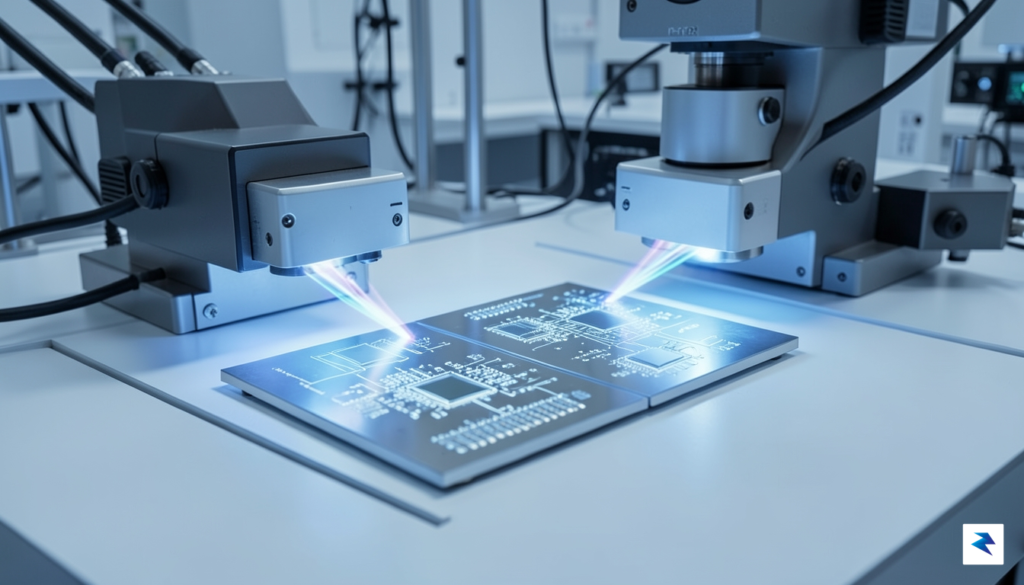
International partnerships and government-backed subsidies serve as the scaffolding for this ambitious expansion, providing the necessary liquidity to navigate the high-stakes environment of semiconductor fabrication. By aligning its production capabilities with the global appetite for sovereign AI and local data center infrastructure, SK Hynix has managed to diversify its risk while deepening its integration into the supply chains of major tech titans. These strategic alliances, coupled with substantial investments in advanced packaging technologies, ensure that the company remains a bottleneck-solver for AI hardware designers who are constantly pushing the limits of bandwidth and thermal management.
For investors, SK Hynix represents a rare ‘pure play’ opportunity: a company whose core revenue stream is inextricably linked to the physical hardware that powers the digital intelligence of the next decade.
Ultimately, the long-term viability of the company hinges on its execution at the intersection of scale and innovation. As the AI landscape matures, the focus will shift from simple capacity to specialized, application-specific memory solutions that can handle the massive computational loads of real-time inferencing. Because SK Hynix has successfully secured its role as a foundational supplier for the leading GPU manufacturers, it is uniquely positioned to benefit from the ongoing build-out of global AI infrastructure. For those looking to capture the value of the AI gold rush, the company offers a compelling case for exposure to the underlying hardware layer that will support the next generation of computing architecture for years to come.
You must be logged in to post a comment.