
Clap On, Clap Off: The True Story Behind the World’s Most Infamous Gadget
The Cultural Phenomenon of The Clapper Before the dawn of the internet or the ubiquity of smartphone-controlled light bulbs, there was a…
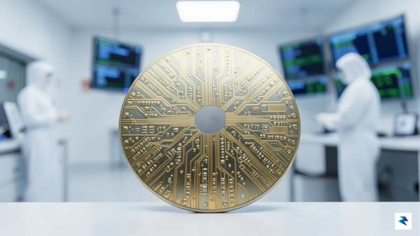
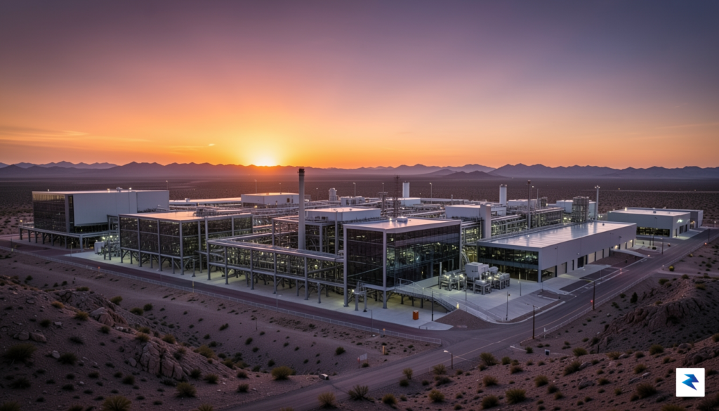
For decades, the global semiconductor industry relied on a highly centralized model, with the vast majority of advanced chip manufacturing concentrated in Taiwan. While this approach enabled TSMC to achieve unparalleled operational efficiency and technical mastery, the vulnerabilities exposed by recent global supply chain disruptions have fundamentally altered the industry’s risk calculus. By committing to a massive $265 billion expansion in Arizona, TSMC is signaling a permanent departure from its traditional geographic limitations, choosing instead to embrace a diversified manufacturing model that prioritizes resilience over pure cost-efficiency.
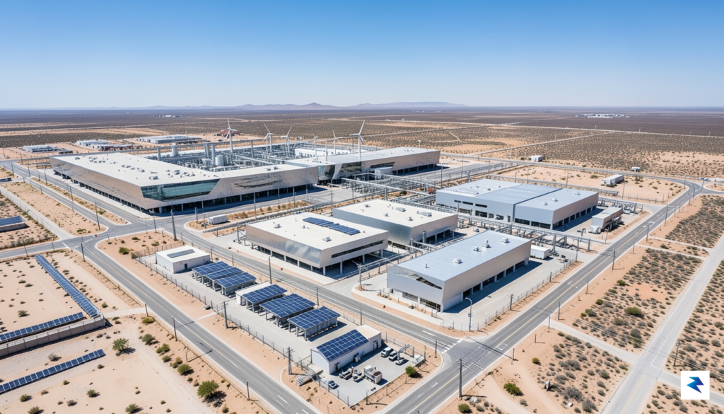
The decision to pour such an astronomical sum into American soil is driven by more than just geopolitical pressure; it is a calculated effort to secure the foundation of the modern digital economy. By establishing four state-of-the-art fabrication plants, or “fabs,” on U.S. territory, TSMC is effectively shortening the distance between its production lines and its most critical customers—the American tech giants that design the world’s most advanced artificial intelligence, cloud computing, and consumer electronics hardware. This proximity reduces logistical bottlenecks and ensures that, should another global crisis emerge, the U.S. domestic supply chain will possess the domestic capacity to sustain its technological momentum without complete reliance on overseas production.
The transition to U.S.-based manufacturing represents a fundamental decoupling of innovation from geography, ensuring that the world’s most critical hardware is produced exactly where its primary demand resides.
Beyond the logistical advantages, this expansion marks a long-term commitment to bridging the domestic manufacturing gap. For years, the United States has led the world in chip design while lagging significantly in high-volume, leading-edge fabrication. This investment directly addresses that imbalance by bringing the most sophisticated lithography and packaging technologies to Arizona, thereby creating a robust ecosystem of specialized labor and infrastructure. As these four fabs come online, they will not only boost U.S. domestic production capacity but will also act as a catalyst for a broader renaissance in domestic hardware engineering, ensuring that the next generation of computing power is both designed and built on American soil.

The aggressive expansion of TSMC’s manufacturing footprint in Arizona represents far more than a simple increase in global production capacity; it functions as a sophisticated geopolitical insurance policy. For decades, the concentration of the world’s most advanced semiconductor fabrication within a relatively small geographic radius in Taiwan has created a precarious single point of failure. By transplanting cutting-edge 2nm and 3nm process nodes to the United States, TSMC is effectively diversifying its operational risk. This strategic migration addresses the vulnerabilities exposed by recent global supply chain disruptions, ensuring that the bedrock of modern technology—the high-performance microchip—remains accessible even if regional instability in the Taiwan Strait were to escalate. This transition from a centralized production model to a geographically distributed one marks a fundamental shift in how the global tech industry views security and continuity.

The economic engine driving this massive capital allocation is primarily fueled by the U.S. CHIPS and Science Act. By providing billions in direct subsidies and investment tax credits, the American government has successfully de-risked the high cost of building and operating fabrication plants on U.S. soil, which traditionally command higher labor and construction expenses compared to East Asian operations. This financial incentive framework has transformed what was once a prohibitively expensive investment into a viable long-term strategy for TSMC. Consequently, this partnership creates a symbiotic relationship: the U.S. secures a domestic supply of critical components necessary for national defense, artificial intelligence, and civilian infrastructure, while TSMC secures a stable, government-backed environment for its next generation of technological growth.
“True supply chain resiliency is not about replacing existing hubs, but about creating redundant, high-capacity nodes that can sustain the global economy during times of localized volatility.”
Furthermore, this expansion does more than just mitigate risk; it actively strengthens the U.S. technology sector by fostering a localized ecosystem of innovation. When advanced manufacturing hubs are established, they naturally attract a constellation of material suppliers, specialized engineering firms, and R&D talent, creating a gravitational pull that revitalizes domestic industrial capabilities. By anchoring these facilities in the Arizona desert, the United States is essentially insulating its technological progress from external shocks. As the global economy continues to shift toward an AI-first paradigm, having these chips forged within domestic borders ensures that the U.S. maintains its competitive edge, shielding its most vital industries from the whims of international trade disputes and geopolitical maneuvering.
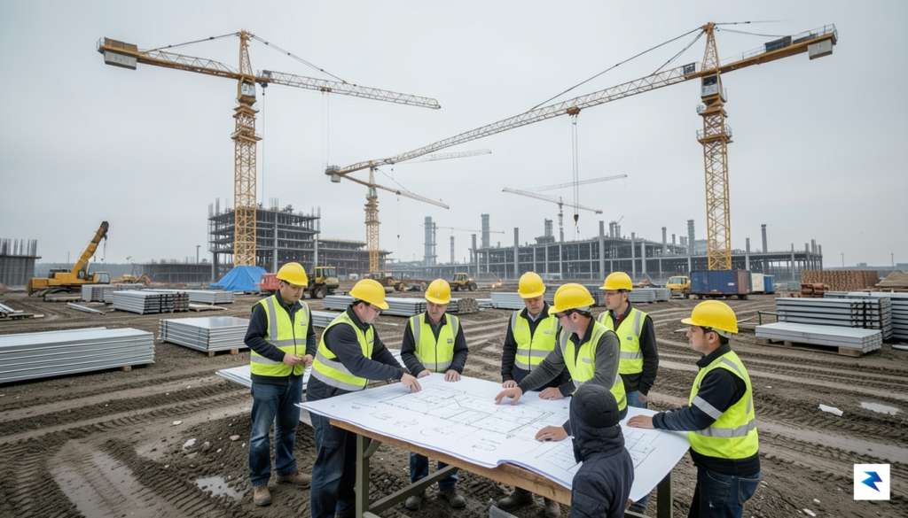
Transforming the Arizona desert into a global epicenter for semiconductor manufacturing is an undertaking of gargantuan proportions, far exceeding the complexity of standard industrial construction. At the heart of this challenge lies a significant labor gap; TSMC is attempting to transplant an ultra-specialized ecosystem that has been refined in Taiwan for decades into an American workforce that currently lacks a deep bench of experienced semiconductor technicians. While the company has invested heavily in training programs and partnerships with local universities, the sheer demand for thousands of engineers who understand the nuances of extreme ultraviolet lithography and complex cleanroom maintenance remains a persistent bottleneck that threatens to slow the pace of deployment.
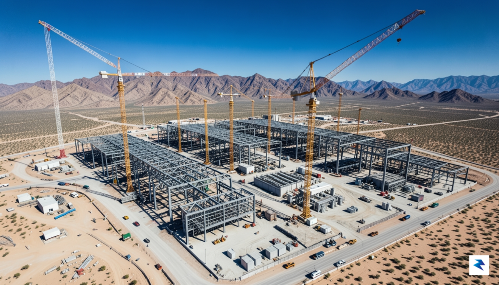
Beyond the human capital crisis, the economic realities of building in the United States present a stark contrast to operations in East Asia. Construction costs in Arizona have ballooned due to a combination of inflationary pressures, supply chain volatility, and the stringent regulatory environment inherent to large-scale American infrastructure projects. TSMC is finding that replicating its “Taiwan speed”—the ability to scale and optimize facilities with surgical precision—is hindered by higher labor rates, complex permitting processes, and the logistical burden of importing specialized equipment from overseas. These financial hurdles mean that every day of delay carries a heavy price tag, forcing the company to balance its ambitious production timelines against the necessity of fiscal discipline.
The integration of advanced chip manufacturing into the domestic landscape is not merely a logistical transition; it is a fundamental test of whether the U.S. can sustain a high-tech manufacturing base that has migrated overseas over the last thirty years.
Furthermore, the physical requirements of modern chip fabrication are immense, placing unprecedented strain on local infrastructure. High-end semiconductor production is notoriously resource-intensive, requiring reliable, ultra-stable power grids and massive volumes of high-purity water to maintain cooling and chemical processing standards. In the arid climate of the American Southwest, securing these utility commitments requires elaborate coordination with local municipalities to ensure that the fabs do not compromise the residential water supply or grid stability. Successfully navigating these hurdles is essential; if TSMC can overcome these systemic barriers, it will not only prove the viability of its $265 billion expansion but also set a new blueprint for how global technology firms can adapt their most critical operations to the unique demands of the North American market.

The relentless surge in artificial intelligence development has transformed high-performance computing (HPC) from a specialized niche into the central pillar of the global tech economy. As giants like Nvidia and Apple push the boundaries of neural network complexity and large language model capabilities, they require a level of computational density that only the most advanced semiconductor nodes can provide. TSMC’s massive $265 billion investment serves as the physical backbone for this digital evolution, ensuring that the silicon substrate necessary for training next-generation AI models is available at scale. Without this expansion, the industry would likely face a sustained bottleneck that could stifle innovation and delay the deployment of mission-critical AI infrastructure.

This expansion is not merely about increasing output; it is about bringing cutting-edge process nodes—such as the 3nm and 2nm technologies—closer to the Western companies that drive AI research. For firms like Apple, which rely on tight integration between hardware and software, having a secure, domestic supply chain for their custom silicon is a strategic imperative rather than a luxury. By localizing production in Arizona, TSMC mitigates the inherent risks associated with global logistics and geopolitical volatility, providing these tech leaders with the stability required for long-term product roadmaps. This proximity allows for faster iteration cycles, enabling engineers to refine chip architectures in real-time as the demands of generative AI continue to shift rapidly.
The integration of localized, high-end fabrication facilities ensures that the United States remains at the forefront of the AI arms race, providing the necessary compute power to maintain a competitive edge in global technological leadership.
Looking toward the future, these new fabs will be instrumental in supporting the next leap in AI training and inference. As models grow in parameter size, the energy efficiency and thermal management of the underlying chips become paramount; TSMC’s Arizona facilities are being built with the specific intent of hosting these highly complex, power-hungry designs. By investing in the infrastructure today, TSMC is laying the groundwork for a future where AI-driven breakthroughs in medicine, climate science, and autonomous systems are no longer limited by chip availability. This commitment effectively bridges the gap between theoretical AI potential and real-world implementation, cementing the role of the American-based fab as a cornerstone of the modern computing era.
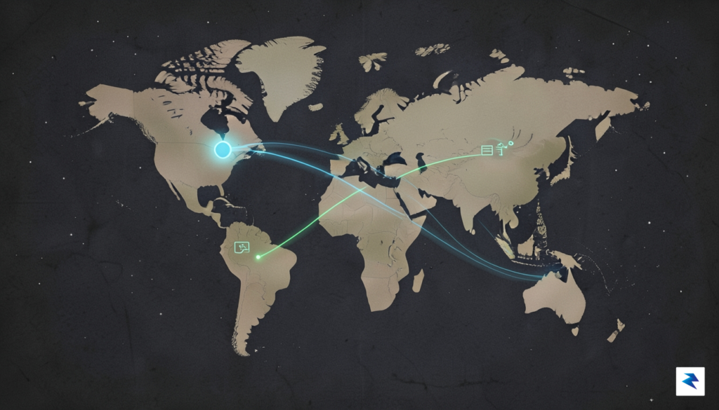
The monumental $265 billion commitment from TSMC marks a definitive shift away from the hyper-centralized manufacturing model that defined the last three decades. For years, the global tech industry operated on a “just-in-time” supply chain that relied heavily on a handful of facilities in Taiwan, leaving the world vulnerable to geopolitical friction and environmental disruptions. By planting deep roots in Arizona, TSMC is effectively architecting a more decentralized, resilient infrastructure. While this transition promises a more robust supply chain capable of weathering future crises, it undeniably comes with a higher price tag. The increased operational costs associated with U.S.-based labor, regulatory compliance, and localized logistics mean that the era of bargain-bin silicon may be drawing to a close, forcing tech businesses to adjust their long-term pricing strategies.
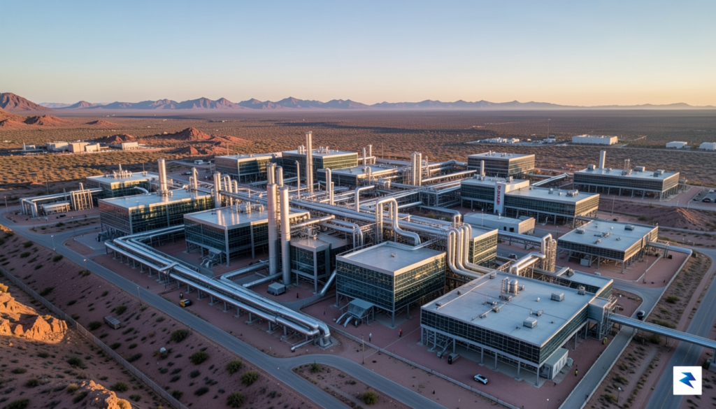
For the average consumer, this pivot suggests a transition toward “premium resilience.” As chip manufacturing costs rise to account for the geographic diversification of production, companies will likely pass these expenses down to the end-user. However, this trade-off provides a vital benefit: a more consistent supply of essential electronics. Rather than facing cyclical shortages of smartphones, laptops, and automotive microcontrollers, the market should see a stabilization of availability. Businesses, in turn, will benefit from a more predictable procurement landscape, allowing for better inventory management and less reliance on the volatile shipping lanes of the Pacific.
The move to domestic manufacturing isn’t just about output; it is about building a buffer against the unpredictability of a hyper-globalized world.
Looking toward the next decade, the partnership between the United States and Taiwan represents a sophisticated model of technological diplomacy. Rather than a total migration of capacity, we are witnessing a symbiotic integration where Taiwan remains the hub for cutting-edge R&D and the most advanced process nodes, while the U.S. facility serves as a secure, high-volume production fortress. This collaboration effectively hedges against localized risks while ensuring that the collaborative spirit of chip innovation continues to thrive. Ultimately, this $265 billion gamble is an investment in stability, signaling that while the cost of entry for the modern digital age is increasing, the security of the underlying infrastructure has become the most valuable commodity of all.
You must be logged in to post a comment.